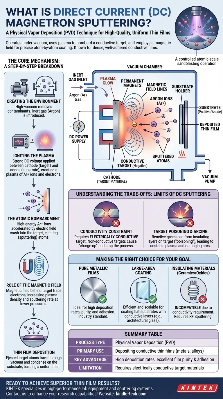
At its core, DC magnetron sputtering is a physical vapor deposition (PVD) technique used to deposit high-quality, uniform thin films onto a substrate. It operates under a vacuum by creating a plasma, using that plasma to bombard a source material (the "target"), and precisely controlling the process with a magnetic field to coat a substrate atom by atom. This method is highly valued for its ability to produce dense, well-adhered films from conductive materials.
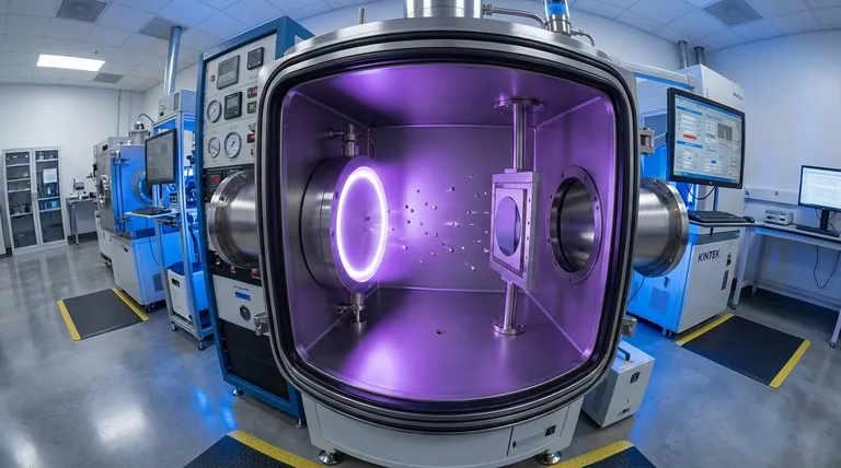
This process can be visualized as a highly controlled, atomic-scale sandblasting operation. Instead of sand, it uses ionized gas (plasma) to chip away atoms from a source material, which then travel through a vacuum and deposit as an ultrathin layer on a component.
The Core Mechanism: A Step-by-Step Breakdown
To truly understand DC magnetron sputtering, we must break it down into its constituent parts. Each step builds upon the last, culminating in the creation of a thin film.
Step 1: Creating the Environment
The entire process takes place within a high-vacuum chamber. This vacuum is critical for two reasons: it removes contaminants that could compromise the film's purity and it allows the sputtered atoms to travel unimpeded from the target to the substrate.
Once a vacuum is achieved, a small, precisely controlled amount of an inert gas, typically argon (Ar), is introduced into the chamber.
Step 2: Igniting the Plasma
A strong Direct Current (DC) voltage is applied between two electrodes: the source material, known as the target, is made the negative electrode (cathode), and the substrate holder or chamber wall acts as the positive electrode (anode).
This high voltage energizes the argon gas, stripping electrons from the argon atoms and creating a mixture of positively charged argon ions (Ar+) and free electrons. This ionized gas is called a plasma, which often emits a characteristic colorful glow.
Step 3: The Atomic Bombardment
The positively charged argon ions are accelerated by the strong electric field and crash into the negatively charged target surface with immense force.
This high-energy collision acts like a subatomic billiard break, ejecting or "sputtering" individual atoms from the target material. These neutral, sputtered atoms now travel through the vacuum chamber.
Step 4: The Role of the Magnetic Field
This is the "magnetron" part of the name and the key innovation. A powerful magnetic field is configured directly behind the target.
This magnetic field does not affect the neutral sputtered atoms, but it traps the lighter, negatively charged electrons from the plasma, forcing them into a spiral path close to the target surface. This electron trap dramatically increases the probability of electrons colliding with and ionizing more argon atoms.
The result is a much denser, more intense plasma concentrated right where it is needed—in front of the target. This significantly increases the sputtering rate and allows the process to operate at lower gas pressures, leading to a higher-purity film.
Step 5: Thin Film Deposition
The ejected target atoms travel through the vacuum until they land on the substrate (the part being coated).
Upon arrival, these atoms condense on the cool substrate surface, gradually building up a thin, dense, and highly uniform film.
Understanding the Trade-offs: The Limits of DC Sputtering
While powerful, the DC magnetron sputtering technique has specific limitations that are crucial to understand.
The Conductivity Constraint
The fundamental requirement for DC sputtering is a constant flow of electrical current. This means the target material must be electrically conductive.
If a non-conductive (dielectric or insulating) target is used, positive charge from the impacting argon ions quickly builds up on its surface. This "charge-up" effect neutralizes the negative voltage and effectively shuts down the sputtering process.
Target Poisoning and Arcing
In some processes, a reactive gas like oxygen or nitrogen is intentionally added to form compound films (e.g., oxides or nitrides). However, this can lead to the formation of an insulating layer on the conductive target itself.
This phenomenon, known as target poisoning, can lead to unstable plasma and destructive arcing events, which can damage the power supply and the quality of the deposited film. For insulating materials, alternative techniques like RF (Radio Frequency) sputtering are required.
Making the Right Choice for Your Goal
DC magnetron sputtering is a foundational technology in thin film deposition, but its application depends entirely on your material and objective.
- If your primary focus is depositing pure metallic films: DC magnetron sputtering is the industry standard, offering high deposition rates, excellent film purity, and superior adhesion.
- If your primary focus is large-area industrial coating (e.g., architectural glass): The efficiency and scalability of DC magnetron sputtering make it an ideal choice for coating large, flat substrates with conductive layers.
- If your primary focus is depositing insulating materials (like ceramics or oxides): You must look to an alternative like RF sputtering, as the fundamental mechanism of DC sputtering is incompatible with non-conductive targets.
By understanding its mechanism and limitations, you can effectively leverage DC magnetron sputtering to achieve exceptionally high-quality thin films.
Summary Table:
| Key Aspect | Description |
|---|---|
| Process Type | Physical Vapor Deposition (PVD) |
| Primary Use | Depositing conductive thin films (metals, alloys) |
| Key Advantage | High deposition rates, excellent film purity and adhesion |
| Limitation | Requires electrically conductive target materials |
| Ideal For | Large-area coatings, industrial applications, and pure metallic films |
Ready to achieve superior thin film results in your lab? KINTEK specializes in high-performance lab equipment and consumables, including sputtering systems designed for precision and reliability. Whether you're coating conductive materials or need expert advice on the right PVD technique for your project, our team is here to help. Contact us today to discuss how our solutions can enhance your laboratory's capabilities and drive your research forward!
Visual Guide
Related Products
- Microwave Plasma Chemical Vapor Deposition MPCVD Machine System Reactor for Lab and Diamond Growth
- Laboratory CVD Boron Doped Diamond Materials
- 915MHz MPCVD Diamond Machine Microwave Plasma Chemical Vapor Deposition System Reactor
- Molybdenum Tungsten Tantalum Special Shape Evaporation Boat
- HFCVD Machine System Equipment for Drawing Die Nano-Diamond Coating
People Also Ask
- What are the primary advantages of the CVD method for growing diamonds? Engineering High-Purity Gems and Components
- How do vacuum pumps and valves collaborate in MPCVD? Achieve Precise Pressure Control for Superior CNT Synthesis
- How does MPCVD work? A Guide to Low-Temperature, High-Quality Film Deposition
- Why is argon-rich gas phase chemistry used for UNCD growth? Unlock Precision Nano-Diamond Synthesis
- How are CVD diamonds created? Discover the Science of Lab-Grown Diamond Precision


