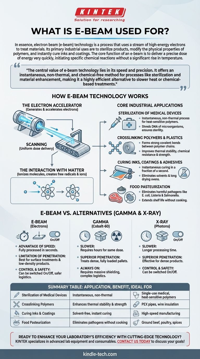
In essence, electron beam (e-beam) technology is a process that uses a stream of high-energy electrons to treat materials. Its primary industrial uses are to sterilize products, modify the physical properties of polymers, and instantly cure inks and coatings. The core function of an e-beam is to deliver a precise dose of energy very quickly, initiating specific chemical reactions without a significant rise in temperature.
The central value of e-beam technology lies in its speed and precision. It offers an instantaneous, non-thermal, and chemical-free method for processes like sterilization and material enhancement, making it a highly efficient alternative to slower heat or chemical-based treatments.
How E-Beam Technology Works
To understand its applications, you must first grasp the core principle. An e-beam accelerator is fundamentally a device that generates, accelerates, and directs a controlled stream of electrons.
The Electron Accelerator
Think of an old cathode-ray tube (CRT) television, but vastly more powerful. A filament is heated, releasing electrons. A series of powerful electric and magnetic fields then grab these electrons and accelerate them to nearly the speed of light, forming a concentrated beam of energy.
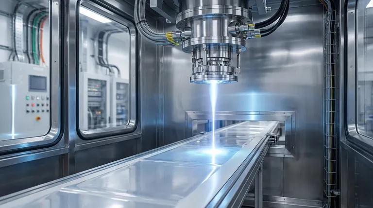
This beam is then scanned across the target material, much like a pencil coloring in a shape, to ensure a uniform dose of energy is applied to the product as it passes by on a conveyor.
The Interaction with Matter
When these high-energy electrons strike a material, they transfer their energy to the atoms and molecules within. This energy transfer primarily ionizes molecules—knocking other electrons out of their orbits. This creates highly reactive free radicals and ions, which in turn drive the desired chemical changes, such as breaking microbial DNA or forming new polymer bonds.
Core Industrial Applications
The unique properties of e-beam—speed, precision, and room-temperature operation—make it the ideal solution for several key industrial challenges.
Sterilization of Medical Devices
E-beam is a dominant method for sterilizing single-use medical devices like syringes, surgical gowns, and implants. Because the process is nearly instantaneous and generates very little heat, it is perfect for treating heat-sensitive polymers and plastics without causing melting or degradation. The electrons effectively shred the DNA of any microorganisms, ensuring sterility even through sealed packaging.
Crosslinking Polymers and Plastics
This is one of e-beam's most powerful applications. When e-beam energy strikes a polymer like polyethylene, it causes adjacent polymer chains to form strong, covalent bonds with each other—a process called crosslinking. This dramatically improves the material's thermal stability, chemical resistance, and physical strength. Common examples include PEX pipes for hot water and specialized insulation for high-performance wires and cables.
Curing Inks, Coatings, and Adhesives
In high-speed manufacturing, e-beam offers instantaneous curing. Specially formulated inks, coatings, or adhesives are applied to a surface and immediately passed under the beam. The energy polymerizes the liquid into a solid, durable layer in a fraction of a second. This process eliminates the need for solvents (improving air quality) and long drying ovens (saving energy and factory floor space).
Food Pasteurization
E-beam processing can be used to pasteurize food products, a process often referred to as food irradiation. It effectively eliminates harmful pathogens like E. coli, Listeria, and Salmonella from ground beef, poultry, and spices. This extends shelf life and improves food safety without cooking the product or leaving any residue.
Understanding the Trade-offs: E-Beam vs. Alternatives
No technology is perfect for every situation. The choice to use e-beam is often made by comparing it to its main alternatives: Gamma irradiation (using Cobalt-60) and X-ray irradiation.
The Advantage of Speed
This is e-beam's defining strength. A product can be fully processed by an e-beam in a matter of seconds. In contrast, gamma irradiation requires exposing products to the radioactive source for several hours to achieve the same sterilizing dose. This makes e-beam ideal for high-volume, low-margin products.
The Limitation of Penetration
Electrons are physical particles with mass, and they are stopped relatively easily by dense materials. This gives e-beam a limited penetration depth. It is perfect for surface treatments, low-density products (like medical foam), or products that can be irradiated from two sides. However, it cannot effectively treat very dense products or fully loaded pallets, where the superior penetration of gamma rays or X-rays is required.
The Matter of Control and Safety
An e-beam accelerator can be switched on and off with a button. When it is off, there is no radiation. A gamma source, however, is a radioisotope that is always emitting radiation. This requires massive, permanent shielding, complex logistics for source replenishment, and significant physical security, making e-beam operationally simpler and safer when not in use.
Making the Right Choice for Your Goal
The decision between e-beam, gamma, or X-ray depends entirely on your product's characteristics and your processing goals.
- If your primary focus is high-volume processing of low-density or surface-treated products: E-beam is almost always the most efficient and cost-effective choice due to its unmatched speed.
- If your primary focus is sterilizing dense, large, or fully palletized products: Gamma or X-ray irradiation is necessary to ensure the energy penetrates completely through the entire product load.
- If your primary focus is on-demand processing and operational simplicity: E-beam's "on/off" capability provides a significant logistical and safety advantage over the "always-on" nature of a gamma source.
By understanding these fundamental trade-offs, you can confidently select the energy-delivery technology that best aligns with your material and business objectives.
Summary Table:
| Application | Key Benefit | Ideal For |
|---|---|---|
| Sterilization of Medical Devices | Instantaneous, non-thermal process | Single-use medical devices, heat-sensitive polymers |
| Crosslinking Polymers | Enhances thermal stability & strength | PEX pipes, wire insulation |
| Curing Inks & Coatings | Solvent-free, instant curing | High-speed manufacturing |
| Food Pasteurization | Eliminates pathogens without cooking | Ground beef, poultry, spices |
Ready to enhance your laboratory's efficiency with cutting-edge technology? KINTEK specializes in providing advanced lab equipment and consumables tailored to your specific needs. Whether you're exploring sterilization methods or material enhancement processes, our expertise can help you achieve superior results. Contact us today to discuss how we can support your laboratory's goals!
Visual Guide
Related Products
- Electron Beam Evaporation Coating Tungsten Crucible and Molybdenum Crucible for High Temperature Applications
- Electron Beam Evaporation Coating Oxygen-Free Copper Crucible and Evaporation Boat
- E Beam Crucibles Electron Gun Beam Crucible for Evaporation
- Electron Beam Evaporation Coating Gold Plating Tungsten Molybdenum Crucible for Evaporation
- Electron Beam Evaporation Coating Conductive Boron Nitride Crucible BN Crucible
People Also Ask
- What is the temperature of e-beam evaporation? Mastering the Two-Zone Thermal Process for Precision Films
- What is the voltage of e-beam evaporation? Achieve Precise Thin-Film Deposition
- What is e-beam evaporation used for? Precision Coating for Optics, Aerospace & Electronics
- What is the deposition rate of e-beam evaporation? Control Thin Film Quality and Speed
- What materials are used in electron beam evaporation? Master High-Purity Thin Film Deposition


