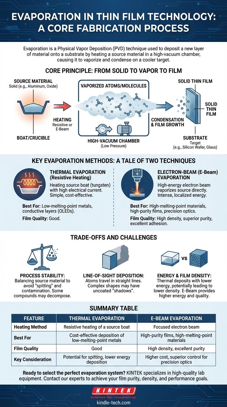
In thin film technology, evaporation is a core fabrication process used to deposit a new layer of material onto a surface, known as a substrate. This is achieved by heating a source material within a high-vacuum chamber until it vaporizes. The resulting atoms or molecules then travel through the vacuum and condense onto the cooler substrate, gradually building up a solid, uniform thin film.
Evaporation is a type of Physical Vapor Deposition (PVD) where heat is the driving force. The crucial decision is not if you use heat, but how you apply it—either through simple resistive heating or a high-energy electron beam—as this choice directly impacts the film's density, purity, and suitability for advanced applications.
The Core Principle: From Solid to Vapor to Film
Evaporation leverages a straightforward physical phase change. By controlling the environment and energy source, we can precisely transfer material from a source to a target.
The Critical Role of the Vacuum
The entire process occurs in a high-vacuum (low-pressure) environment. This is non-negotiable for two reasons: it prevents the vaporized material from reacting with air, ensuring film purity, and it allows the atoms to travel in a straight line from the source to the substrate without colliding with other gas molecules.
The Source and The Substrate
The source material is the substance you wish to deposit, such as a pure metal like aluminum or a compound like an oxide. This material is placed in a holder, often called a "boat" or "crucible." The substrate is the target object being coated, which could be a silicon wafer, a piece of glass, or a flexible polymer.
Condensation and Film Growth
As the vapor cloud of atoms reaches the relatively cool substrate, it rapidly loses its energy and condenses back into a solid state. Atom by atom, layer by layer, this condensation process grows the desired thin film.
Key Evaporation Methods: A Tale of Two Techniques
While the principle is the same, the method used to heat the source material defines the two primary types of evaporation.
Thermal Evaporation (Resistive Heating)
This is the classic form of evaporation. The source material is placed in a small container, or "boat," typically made of a refractory metal like tungsten. A high electrical current is passed through this boat, causing it to heat up resistively—much like the filament in an incandescent light bulb. This heat is transferred to the source material, causing it to evaporate.
This method is simple and cost-effective, making it ideal for depositing pure metals with relatively low melting points, such as the electrically conductive layers in OLED displays or thin-film transistors.
Electron-Beam (E-Beam) Evaporation
For materials with very high melting points or for applications demanding higher purity, e-beam evaporation is the superior choice. In this technique, a high-energy beam of electrons is generated and magnetically guided to strike the source material directly.
This intense, localized energy can vaporize virtually any material without heating the entire chamber. The result is a higher-purity vapor and, consequently, a higher-density thin film with excellent adhesion to the substrate. This control is critical for producing precision laser optics and specialized architectural glass.
Understanding the Trade-offs and Challenges
While powerful, evaporation is a process with inherent limitations that must be managed for successful film deposition.
Process Stability and Material Behavior
Maintaining a perfectly stable evaporation rate can be challenging. A common issue involves balancing the amount of material in the source; too much can lead to "spitting," where small solid particles are ejected and contaminate the film. Furthermore, some compounds can decompose or react when heated, altering the composition of the final film.
Line-of-Sight Deposition
Evaporation is a line-of-sight process. Atoms travel in straight lines from the source to the substrate. This means that any part of the substrate not in the direct path of the vapor—such as the sides of a complex 3D object—will not get coated, creating a "shadow."
Energy and Film Density
Simple thermal evaporation deposits atoms with relatively low energy. This can sometimes result in films that are less dense or have weaker adhesion compared to those produced by e-beam evaporation or other PVD methods like sputtering. E-beam provides more energy, leading to higher-quality films.
Making the Right Choice for Your Application
Selecting the correct deposition method requires matching the technique's strengths to your end goal.
- If your primary focus is cost-effective deposition of simple metals: Thermal evaporation is often the most direct and economical solution for applications like basic conductive coatings.
- If your primary focus is high-purity, dense films or optical coatings: E-beam evaporation offers superior control, enabling the deposition of complex materials and the creation of precision optics.
- If your primary focus is uniform coating on complex, non-flat shapes: You may need to look beyond evaporation to a process like sputtering or chemical vapor deposition (CVD) to overcome line-of-sight limitations.
By understanding these core principles and trade-offs, you are empowered to select the precise deposition strategy for your specific technical goal.
Summary Table:
| Feature | Thermal Evaporation | E-Beam Evaporation |
|---|---|---|
| Heating Method | Resistive heating of a source boat | Focused electron beam |
| Best For | Cost-effective deposition of low-melting-point metals | High-purity films, high-melting-point materials |
| Film Quality | Good | High density, excellent purity |
| Key Consideration | Potential for spitting, lower energy deposition | Higher cost, superior control for precision optics |
Ready to select the perfect evaporation system for your lab's thin film needs? KINTEK specializes in high-quality lab equipment, including thermal and e-beam evaporation systems. Our experts can help you choose the right PVD solution to achieve the film purity, density, and performance your research demands. Contact our team today to discuss your specific application!
Visual Guide
Related Products
- Molybdenum Tungsten Tantalum Evaporation Boat for High Temperature Applications
- Aluminized Ceramic Evaporation Boat for Thin Film Deposition
- Evaporation Boat for Organic Matter
- Chemical Vapor Deposition CVD Equipment System Chamber Slide PECVD Tube Furnace with Liquid Gasifier PECVD Machine
- Multi Heating Zones CVD Tube Furnace Machine Chemical Vapor Deposition Chamber System Equipment
People Also Ask
- What is the source of evaporation for thin film? Choosing Between Thermal and E-Beam Methods
- How source material is evaporated during deposition? A Guide to Resistive vs. E-Beam Methods
- What is thermal evaporation used to deposit? A Guide to Metals, Compounds, and Key Applications
- What is the widely used boat made of in thermal evaporation? Choosing the Right Material for High-Purity Deposition
- What are thermal evaporation sources? Key Types and How to Choose the Right One