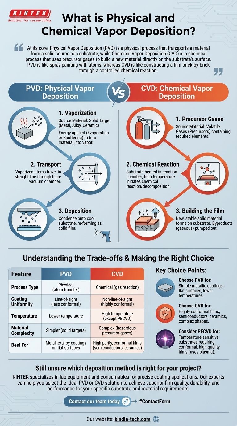
At its core, Physical Vapor Deposition (PVD) is a physical process that transports a material from a solid source to a substrate, while Chemical Vapor Deposition (CVD) is a chemical process that uses precursor gases to build a new material directly on the substrate's surface. PVD is like spray painting with atoms, whereas CVD is like constructing a film brick-by-brick through a controlled chemical reaction.
The fundamental distinction is simple: PVD moves an existing solid material from one place to another. CVD uses chemical reactions between gases to create an entirely new solid material on a surface.
The Mechanism of Physical Vapor Deposition (PVD)
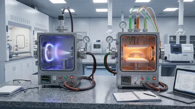
Physical Vapor Deposition is a line-of-sight process that involves three main steps: vaporization, transport, and deposition. The entire process occurs within a high-vacuum chamber to ensure the purity of the final film.
The Source Material
The process begins with a solid piece of the material you wish to deposit, known as the "target" or "source." This could be a pure metal, an alloy, or a ceramic.
The Vaporization Process
Energy is applied to the source material to turn it into a vapor. This is achieved through purely physical means, most commonly through evaporation (heating the material until it boils) or sputtering (bombarding the material with high-energy ions, which knocks atoms loose).
The Deposition Step
These vaporized atoms travel in a straight line through the vacuum chamber and condense onto the cooler substrate. This condensation re-forms the material as a thin, solid film on the substrate’s surface.
The Mechanism of Chemical Vapor Deposition (CVD)
Chemical Vapor Deposition is a more complex process that relies on a chemical reaction to form the coating. It is not limited by a line-of-sight, allowing it to coat intricate shapes uniformly.
The Precursor Gases
CVD begins not with a solid, but with one or more volatile gases known as "precursors." These gases contain the chemical elements required to form the final film.
The Chemical Reaction
The substrate is placed in a reaction chamber and heated. The precursor gases are then introduced into the chamber, where the high temperature provides the energy needed for them to react or decompose on the substrate's hot surface.
Building the Film
This chemical reaction forms a new, stable solid material directly on the substrate. The reaction byproducts, which are typically gaseous, are then pumped out of the chamber. The process effectively "grows" the desired film on the surface.
Understanding the Trade-offs
Choosing between PVD and CVD requires understanding their inherent limitations and advantages. The right choice depends entirely on the material, the substrate, and the desired properties of the final film.
PVD: Line-of-Sight Limitation
Because the vaporized atoms in PVD travel in a straight line, it can be difficult to achieve a uniform coating on complex, three-dimensional parts. Surfaces not in the direct line of sight of the source material will receive little to no coating.
CVD: High-Temperature Requirement
Traditional thermal CVD processes require very high temperatures to initiate the necessary chemical reactions. This heat can easily damage temperature-sensitive substrates, such as plastics or certain electronic components.
CVD: Process and Material Complexity
The chemistry involved in CVD can be complex and hazardous. The precursor gases are often toxic, corrosive, or pyrophoric, requiring specialized handling and equipment. In contrast, PVD often works with stable, solid source materials.
PVD vs. CVD: Film Conformance
CVD excels at creating highly conformal coatings, meaning the film's thickness is perfectly uniform across even the most complex topographies. Because PVD is a line-of-sight process, its ability to conform to surfaces is significantly lower.
Making the Right Choice for Your Goal
Your application's specific requirements will dictate which method is superior. The decision hinges on the trade-off between process simplicity, temperature constraints, and the desired quality of the final film.
- If your primary focus is depositing a simple metallic or alloy coating on a relatively flat surface: PVD is often the more direct, cost-effective, and lower-temperature solution.
- If your primary focus is creating an exceptionally pure, dense, and highly conformal film (like a semiconductor or ceramic): CVD's chemical growth process is typically the superior choice, provided the substrate can withstand the heat.
- If your substrate is temperature-sensitive but requires a conformal, high-quality film: You should investigate lower-temperature CVD variants, such as Plasma-Enhanced CVD (PECVD), which uses plasma instead of high heat to drive the reaction.
Ultimately, understanding the fundamental difference between physical transport and chemical creation is the key to selecting the ideal deposition technology for your application.
Summary Table:
| Feature | PVD (Physical Vapor Deposition) | CVD (Chemical Vapor Deposition) |
|---|---|---|
| Process Type | Physical (atom transfer) | Chemical (gas reaction) |
| Coating Uniformity | Line-of-sight (less conformal) | Non-line-of-sight (highly conformal) |
| Temperature | Lower temperature | High temperature (except PECVD) |
| Material Complexity | Simpler (solid targets) | Complex (hazardous precursor gases) |
| Best For | Metallic/alloy coatings on flat surfaces | High-purity, conformal films (semiconductors, ceramics) |
Still unsure which deposition method is right for your project?
KINTEK specializes in lab equipment and consumables for precise coating applications. Our experts can help you select the ideal PVD or CVD solution to achieve superior film quality, durability, and performance for your specific substrate and material requirements.
Contact our team today for a personalized consultation and discover how KINTEK can enhance your laboratory's capabilities!
Visual Guide
Related Products
- Chemical Vapor Deposition CVD Equipment System Chamber Slide PECVD Tube Furnace with Liquid Gasifier PECVD Machine
- RF PECVD System Radio Frequency Plasma-Enhanced Chemical Vapor Deposition RF PECVD
- 915MHz MPCVD Diamond Machine Microwave Plasma Chemical Vapor Deposition System Reactor
- HFCVD Machine System Equipment for Drawing Die Nano-Diamond Coating
- Split Chamber CVD Tube Furnace with Vacuum Station Chemical Vapor Deposition System Equipment Machine
People Also Ask
- What is plasma enhanced chemical vapor deposition PECVD equipment? A Guide to Low-Temperature Thin Film Deposition
- How expensive is chemical vapor deposition? Understanding the True Cost of High-Performance Coating
- What types of substrates are used in CVD to facilitate graphene films? Optimize Graphene Growth with the Right Catalyst
- What are the advantages of chemical vapor deposition? Achieve Superior Thin Films for Your Lab
- What are the core advantages of PE-CVD in OLED encapsulation? Protect Sensitive Layers with Low-Temp Film Deposition


