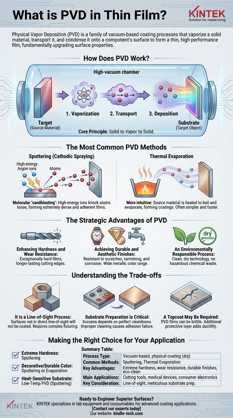
In the context of thin films, PVD stands for Physical Vapor Deposition. It is a family of vacuum-based coating processes where a solid material is vaporized, transported through the vacuum, and condensed onto a component's surface to form a thin, high-performance film. This allows you to give an object the surface properties of one material while retaining the bulk properties (like cost or weight) of another.
Physical Vapor Deposition is not a single technique but a versatile engineering toolkit. It is used to strategically apply a very thin layer of material to a surface, fundamentally changing its properties like hardness, wear resistance, or color, without altering the underlying component.
How Does PVD Work?
PVD processes, despite their variations, all follow the same fundamental sequence within a high-vacuum chamber. This controlled environment is crucial for ensuring the purity and quality of the final film.
The Core Principle: Solid to Vapor to Solid
The entire process involves three key stages:
- Vaporization: A solid source material, known as the "target," is converted into a vapor.
- Transport: The vaporized atoms or molecules travel in a straight line through the vacuum chamber.
- Deposition: The vapor condenses onto the cooler target object (the "substrate"), forming a thin, dense, and tightly bonded film.
The Most Common PVD Methods
While there are many PVD techniques, two are predominant for their versatility and commercial use.
Sputtering (Cathodic Spraying)
Sputtering can be visualized as a form of molecular "sandblasting." In this method, high-energy ions (typically from an inert gas like argon) are accelerated and aimed at the target material. The impact of these ions physically knocks atoms loose from the target, which then travel and deposit onto the substrate.
Sputtering is highly valued for producing extremely dense and adherent films, making it a preferred method for demanding applications.
Thermal Evaporation
Thermal evaporation is a more intuitive process. The source material is heated in the vacuum chamber until it begins to boil and evaporate, releasing a vapor. This vapor then travels to the substrate and condenses back into a solid, forming the coating.
This method is often simpler and faster than sputtering, but the resulting films may be less dense.
The Strategic Advantages of PVD
PVD is used because it solves critical engineering and design challenges by fundamentally upgrading a surface.
Enhancing Hardness and Wear Resistance
PVD films can be exceptionally hard, often many times harder than steel. As noted in the metal cutting industry, this has revolutionized tools like drills, end mills, and thread cutters.
A PVD coating provides a tough, low-friction cutting edge that stays sharp far longer, enabling higher speeds and superior performance on difficult materials.
Achieving Durable and Aesthetic Finishes
PVD is used extensively for decorative purposes where durability is paramount. It can produce a wide range of metallic colors (gold, black, bronze, rose gold) on products like watches, faucets, and hardware.
Unlike paint or traditional plating, these PVD finishes are highly resistant to scratches, tarnishing, and corrosion.
An Environmentally Responsible Process
Compared to traditional wet-chemical processes like electroplating, PVD is a dry, environmentally clean technology. It does not produce the hazardous chemical waste associated with many older coating methods.
Understanding the Trade-offs
While powerful, PVD is a precise engineering process with specific limitations that must be understood for successful application.
It Is a Line-of-Sight Process
Because the vaporized material travels in a straight line, surfaces not in the direct "line of sight" of the source will not be coated. Coating complex, three-dimensional parts requires sophisticated fixtures that rotate the parts during the process to ensure uniform coverage.
Substrate Preparation is Critical
The success of a PVD coating is entirely dependent on the cleanliness of the substrate. The surface must be perfectly free of oils, oxides, and any other contaminants. Improper cleaning is the most common cause of coating adhesion failure.
A Topcoat May Be Required
While PVD films are extremely hard, they can also be brittle. For applications subject to impact or significant abrasion, an additional protective layer may be applied. A clear powder coating, for instance, can provide a more ductile outer layer that protects the PVD film from damage while maintaining its high-gloss appearance.
Making the Right Choice for Your Application
The decision to use PVD—and which method to choose—depends entirely on your end goal.
- If your primary focus is extreme hardness and wear resistance for industrial tools: Sputtering is often the superior choice for its ability to create dense, highly adherent films that withstand intense stress.
- If your primary focus is a decorative, durable color on consumer goods: Both sputtering and evaporation are effective, with the final choice depending on the specific material, desired finish, and cost considerations.
- If your primary focus is coating a heat-sensitive substrate like plastic: You must select a low-temperature PVD process, where sputtering often has an advantage over high-heat evaporation.
Ultimately, PVD empowers you to engineer a surface with precisely the properties you need, unlocking new levels of performance and design that the base material alone could never achieve.
Summary Table:
| Key Aspect | Details |
|---|---|
| Process Type | Vacuum-based, physical coating (dry process) |
| Common Methods | Sputtering, Thermal Evaporation |
| Key Advantages | Extreme hardness, wear resistance, durable decorative finishes, environmentally clean |
| Main Applications | Cutting tools, medical devices, consumer electronics, wear-resistant components |
| Key Consideration | Line-of-sight process; requires meticulous substrate preparation |
Ready to Engineer Superior Surfaces?
PVD technology can transform your product's performance, durability, and aesthetics. Whether you need to enhance the wear resistance of industrial tools or achieve a lasting, brilliant finish on consumer goods, KINTEK has the expertise and equipment to help.
We specialize in providing lab equipment and consumables for advanced coating applications. Contact our experts today to discuss how PVD can solve your specific challenges and add value to your products.
Visual Guide
Related Products
- RF PECVD System Radio Frequency Plasma-Enhanced Chemical Vapor Deposition RF PECVD
- Evaporation Boat for Organic Matter
- Molybdenum Tungsten Tantalum Evaporation Boat for High Temperature Applications
- Hemispherical Bottom Tungsten Molybdenum Evaporation Boat
- Chemical Vapor Deposition CVD Equipment System Chamber Slide PECVD Tube Furnace with Liquid Gasifier PECVD Machine
People Also Ask
- What are the applications of PECVD? Essential for Semiconductors, MEMS, and Solar Cells
- What is an example of PECVD? RF-PECVD for High-Quality Thin Film Deposition
- What are the advantages of PECVD? Enable Low-Temperature, High-Quality Thin-Film Deposition
- What is the principle of plasma enhanced chemical vapor deposition? Achieve Low-Temperature Thin Film Deposition
- Why does PECVD commonly use RF power input? For Precise Low-Temperature Thin Film Deposition