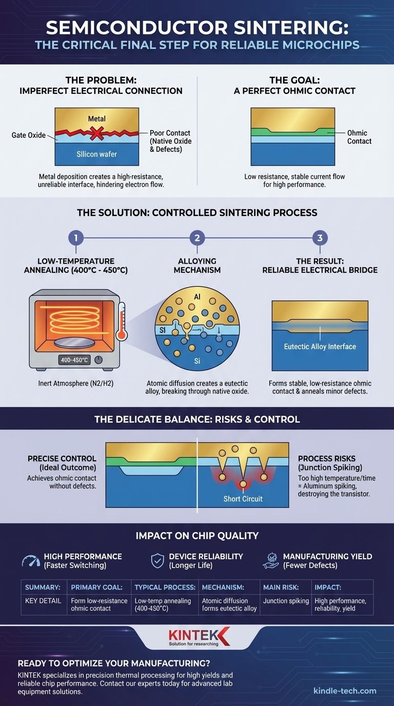
In semiconductors, sintering is a specific, low-temperature annealing step performed after metal layers have been deposited onto the silicon wafer. Its primary purpose is not to compact a powder, but to form a high-quality, low-resistance electrical connection—known as an ohmic contact—between the metal and the underlying silicon.
The core problem is that simply placing metal on silicon creates a poor, unreliable electrical connection. Sintering is the critical final heating process that alloys these two materials at their interface, clearing the way for electrons to flow efficiently and ensuring the microchip functions correctly.
The Problem: An Imperfect Connection
To understand why sintering is essential, we first need to appreciate the challenge it solves in chip manufacturing.
The Challenge of Metallization
After transistors are built into the silicon, thin layers of metal, typically aluminum or copper, are deposited to act as wires, connecting the transistors to each other and to the outside world.
However, just depositing this metal layer doesn't guarantee a good electrical contact. A microscopic, insulating layer of native oxide can get trapped at the interface, and the deposition process itself can create defects in the silicon surface.
The Goal: A Perfect "Ohmic Contact"
The ideal connection is an ohmic contact. This is a junction with extremely low electrical resistance that allows current to flow equally well in both directions without significant voltage drop.
Without an ohmic contact, the performance of the transistor is severely compromised. The high resistance acts like a bottleneck for electrons, slowing the chip down and wasting power as heat.
How Sintering Creates the Solution
Sintering is a carefully controlled heating process that transforms this imperfect junction into a near-perfect ohmic contact.
The Process: Low Temperature, High Impact
A completed silicon wafer is placed in a furnace and heated to a relatively low temperature, typically between 400°C and 450°C. This is well below the melting point of aluminum (660°C) and silicon (1414°C).
This heating is done in an inert or "forming gas" atmosphere (a mix of nitrogen and hydrogen) to prevent oxidation.
The Mechanism: Alloying at the Interface
At this elevated temperature, atomic diffusion begins. A small amount of the silicon from the wafer dissolves into the solid aluminum layer at the point of contact.
Simultaneously, some aluminum atoms diffuse a tiny distance into the silicon. This process effectively breaks through any residual native oxide layer that was blocking the connection.
The Result: A Reliable Electrical Bridge
As the wafer cools, this mixture of aluminum and silicon solidifies into a eutectic alloy. This newly formed alloy interface acts as a perfect electrical bridge, creating the stable, low-resistance ohmic contact required for high performance.
A secondary benefit is that this heat treatment also helps anneal, or repair, minor damage to the silicon crystal lattice and the critical gate oxide layer that may have occurred during previous manufacturing steps.
Understanding the Trade-offs and Risks
While essential, the sintering process is a delicate balancing act. The parameters must be controlled with extreme precision.
The Danger of "Junction Spiking"
The most significant risk is aluminum spiking. If the sintering temperature is too high or held for too long, the aluminum can diffuse too deeply into the silicon.
In modern transistors, the active junctions are extremely shallow. The aluminum can "spike" right through this shallow junction, creating an electrical short circuit and destroying the transistor.
The Importance of Process Control
Because of this risk, process engineers must precisely control the sintering temperature and duration. The goal is to achieve a perfect ohmic contact without creating yield-killing defects like junction spiking. This is a classic example of the narrow process windows that define semiconductor manufacturing.
Making the Right Choice for Your Goal
Sintering is not an optional "nice-to-have" step; it is a fundamental requirement for building functional integrated circuits. Its impact is felt across every measure of a chip's quality.
- If your primary focus is high performance: Proper sintering is key, as it minimizes contact resistance, which directly enables faster transistor switching speeds and reduces power consumption.
- If your primary focus is device reliability: The stable, alloyed contact formed during sintering prevents electrical properties from degrading over the chip's lifetime.
- If your primary focus is manufacturing yield: Precisely controlled sintering is critical for avoiding fatal defects like junction spiking, ensuring that a maximum number of chips on a wafer function correctly.
Ultimately, this carefully controlled heating process transforms a simple metal deposit into the functional, reliable electrical heart of every microchip.
Summary Table:
| Aspect | Key Detail |
|---|---|
| Primary Goal | Form a low-resistance ohmic contact between metal and silicon. |
| Typical Process | Low-temperature annealing (400°C - 450°C) in an inert atmosphere. |
| Key Mechanism | Atomic diffusion creates a eutectic alloy at the interface. |
| Main Risk | Junction spiking if temperature/duration is not precisely controlled. |
| Impact on Chips | Enables high performance, reliability, and manufacturing yield. |
Ready to Optimize Your Semiconductor Manufacturing Process?
Precision thermal processing is critical for achieving high yields and reliable chip performance. KINTEK specializes in advanced lab equipment, including furnaces designed for precise sintering and annealing applications.
Our solutions help you:
- Achieve perfect ohmic contacts with precise temperature control.
- Minimize risks like junction spiking for higher yields.
- Ensure the reliability and longevity of your semiconductor devices.
Let KINTEK's expertise in laboratory equipment support your innovation. Contact our thermal processing experts today to discuss your specific semiconductor manufacturing needs.
Visual Guide