Sputter equipment is a highly controlled system used for a process called physical vapor deposition (PVD). At its core, this machinery uses energized ions in a vacuum to knock atoms off a source material—like a microscopic sandblaster—and deposit them as an ultra-thin film onto a substrate. This technique is fundamental to manufacturing countless modern technologies, from microchips to eyeglasses.
Sputtering isn't about melting or painting a surface; it's a precise atomic-level transfer process. Sputter equipment creates a high-vacuum environment where a plasma "sandblasts" a target material, allowing you to deposit a perfectly uniform, ultra-thin layer of that material onto virtually any substrate.
How Sputtering Fundamentally Works
To understand the equipment, you must first understand the process it facilitates. The operation can be broken down into a clear sequence of events.
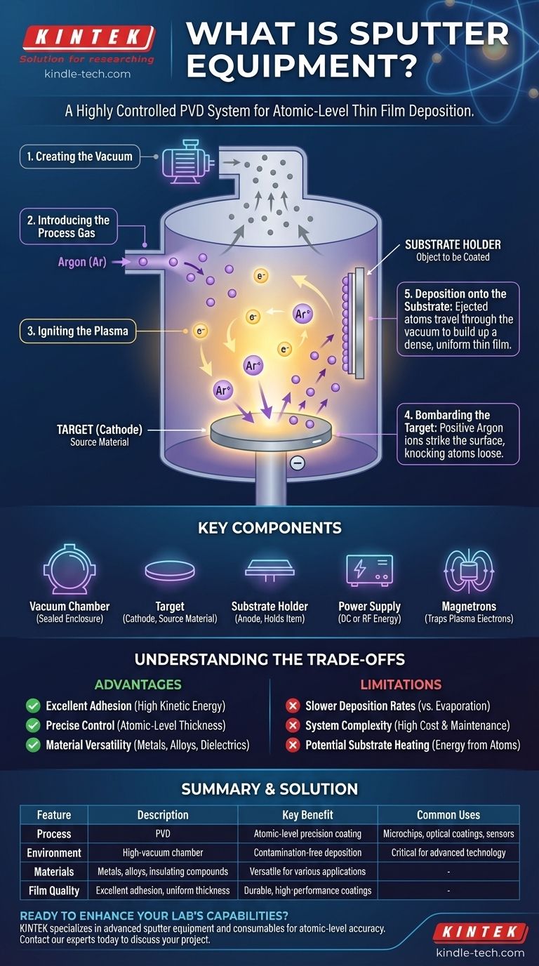
1. Creating the Vacuum
First, a series of pumps removes almost all the air from a sealed process chamber. This is critical to prevent the sputtered atoms from colliding with air molecules and to avoid contamination of the thin film.
2. Introducing the Process Gas
A small, precisely controlled amount of an inert gas, typically Argon (Ar), is then introduced into the chamber. This gas is what will eventually be used to bombard the source material.
3. Igniting the Plasma
A high voltage is applied within the chamber, stripping electrons from the Argon gas atoms. This creates a glowing, energized state of matter known as plasma, which consists of positive Argon ions (Ar+) and free electrons.
4. Bombarding the Target
The source material, known as the target, is given a negative electrical charge. This causes the positive Argon ions from the plasma to accelerate violently towards it, striking its surface with significant energy.
5. Deposition onto the Substrate
Each impact of an Argon ion has enough force to knock atoms loose from the target material. These ejected atoms travel through the vacuum chamber and land on the surface of the object being coated, known as the substrate, gradually building up a dense and uniform thin film.
Key Components of a Sputter System
While designs vary, nearly all sputter deposition systems are built around a core set of components that manage this atomic-scale process.
The Vacuum Chamber
This is the sealed enclosure where the entire process takes place. It's typically made of stainless steel and is engineered to withstand deep vacuum conditions.
The Target (Cathode)
This is a plate made of the material you wish to deposit. It is connected to the negative output of the power supply, making it the "cathode."
The Substrate Holder (Anode)
This platform holds the item to be coated (the wafer, lens, etc.). It is often grounded or positively charged (the "anode") and can frequently be rotated or heated to improve film uniformity and quality.
The Power Supply (DC vs. RF)
The power supply provides the energy to create and sustain the plasma.
- DC (Direct Current) supplies are used for sputtering electrically conductive target materials, like metals.
- RF (Radio Frequency) supplies are required for non-conductive (insulating) materials to prevent charge buildup on the target that would otherwise stop the process.
Magnetrons
Most modern systems are magnetron sputtering systems. They use powerful magnets placed behind the target to trap the plasma's electrons in a magnetic field directly in front of the target. This dramatically increases the number of Argon ions created, leading to a much faster and more efficient deposition rate.
Understanding the Trade-offs
Sputtering is a powerful and versatile technique, but like any engineering process, it involves a series of trade-offs.
Advantages of Sputtering
Excellent Adhesion: Sputtered atoms arrive at the substrate with high kinetic energy, which helps them form a very strong, dense bond with the surface.
Precise Control: The process allows for extremely fine control over film thickness, often down to the single-angstrom level.
Material Versatility: A vast range of materials can be sputtered, including pure metals, alloys, and—with RF power—insulating compounds.
Common Limitations and Challenges
Slower Deposition Rates: Compared to some other methods like thermal evaporation, sputtering can be a slower process, which can impact manufacturing throughput.
System Complexity: Sputter equipment is mechanically and electronically complex, involving high-voltage power, vacuum systems, and gas handling, which translates to higher cost and maintenance.
Potential for Substrate Heating: The energy from the arriving atoms can heat the substrate, which may be undesirable for heat-sensitive materials.
Making the Right Choice for Your Goal
Understanding the strengths of sputtering helps determine if it aligns with your technical requirements for creating a thin film.
- If your primary focus is material purity and strong adhesion: Sputtering is an excellent choice due to the physical bonding mechanism and the clean vacuum environment.
- If your primary focus is depositing a non-conductive (dielectric) material: You will need a system equipped with an RF power supply to handle insulating targets.
- If your primary focus is high throughput for a simple metal coating: You might compare sputtering with thermal evaporation, which can offer higher deposition rates for certain materials.
- If your primary focus is creating a compound film (e.g., an oxide or nitride): You should investigate reactive sputtering, a variation where a reactive gas like oxygen or nitrogen is added to the chamber.
Ultimately, sputter equipment provides an atomic-level construction tool, enabling the precise engineering of surfaces that drive modern technology.
Summary Table:
| Feature | Description | Key Benefit |
|---|---|---|
| Process | Physical Vapor Deposition (PVD) | Atomic-level precision coating |
| Environment | High-vacuum chamber with inert gas | Contamination-free deposition |
| Materials | Metals, alloys, insulating compounds | Versatile for various applications |
| Film Quality | Excellent adhesion, uniform thickness | Durable, high-performance coatings |
| Common Uses | Microchips, optical coatings, sensors | Critical for advanced technology |
Ready to enhance your lab's capabilities with precision thin film deposition?
KINTEK specializes in advanced sputter equipment and consumables, serving laboratories that demand atomic-level accuracy for semiconductors, research, and material science. Our systems deliver the excellent adhesion, material versatility, and precise control your projects require.
Contact our experts today to discuss how our sputtering solutions can accelerate your innovation and achieve superior coating results.
Visual Guide
Related Products
- Professional Cutting Tools for Carbon Paper Cloth Diaphragm Copper Aluminum Foil and More
- Chemical Vapor Deposition CVD Equipment System Chamber Slide PECVD Tube Furnace with Liquid Gasifier PECVD Machine
- HFCVD Machine System Equipment for Drawing Die Nano-Diamond Coating
People Also Ask
- What are the typical uses for carbon paper? Powering Fuel Cells and Advanced Research
- What are the material properties of carbon paper? Unlocking High Conductivity & Porosity for Your Lab
- How should carbon paper be handled during cutting? Prevent Fractures with a Delicate, Precise Approach
- How is carbon paper constructed? The Engineered Porous Scaffold for High-Performance Applications
- What are carbon cloths used for? Conquer Static Dust on Electronics & Screens


