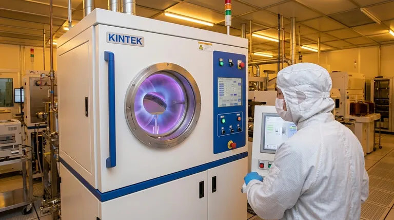
In semiconductor manufacturing, sputtering is a cornerstone process used for physical vapor deposition (PVD). It is a highly controlled method of depositing ultra-thin, exceptionally pure films of material onto a substrate, such as a silicon wafer. This is achieved by bombarding a source material (the "target") with high-energy ions, which physically knock atoms off the target's surface, allowing them to travel and condense onto the wafer.
Sputtering is more than a simple coating technique; it is a precision atomic-scale construction method. Its fundamental value in semiconductor fabrication lies in its ability to deposit a vast range of materials—from conductors to insulators—with the extreme purity and uniformity required to build complex, multi-layered integrated circuits.
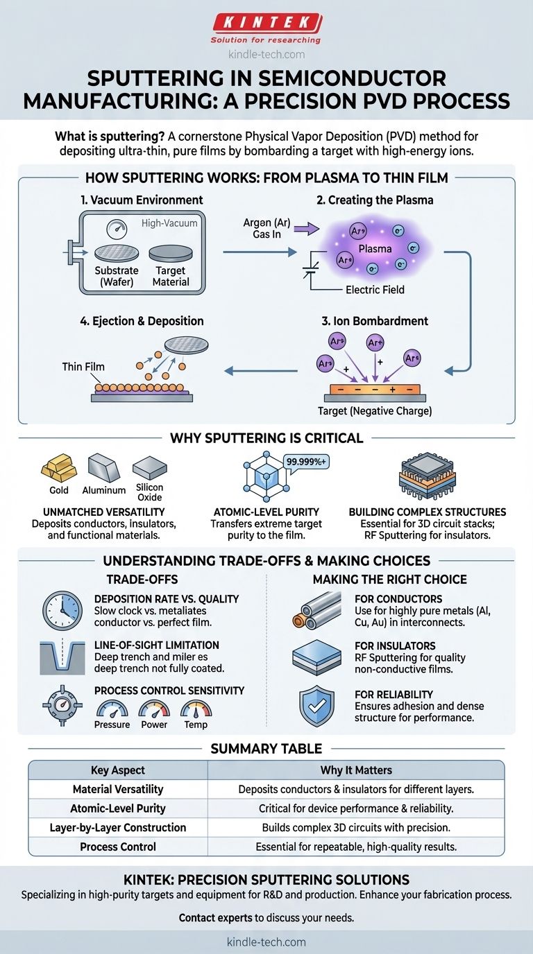
How Sputtering Works: From Plasma to Thin Film
Sputtering is a physical process that takes place inside a vacuum chamber. Understanding the step-by-step mechanism reveals why it is so powerful for creating microscopic electronic structures.
The Vacuum Environment
First, the substrate (the wafer) and the target material are placed in a high-vacuum chamber. This step is critical to remove atmospheric gases and other contaminants that could otherwise be incorporated into the thin film and ruin the semiconductor device.
Creating the Plasma
Next, a small amount of an inert gas, almost always Argon (Ar), is introduced into the chamber. A strong electric or electromagnetic field is then applied, which ionizes the gas. This creates a plasma, a state of matter consisting of positively charged Argon ions (Ar+) and free electrons.
The Target and Ion Bombardment
The material to be deposited—such as gold, aluminum, or tantalum oxide—is shaped into a "target" and given a strong negative electrical charge. The positively charged Argon ions in the plasma are naturally attracted to and accelerate towards this negatively charged target at high speed.
Ejection and Deposition
When these high-energy ions collide with the target, they transfer their momentum and energy, physically knocking out, or "sputtering," individual atoms from the target's surface. These ejected atoms travel through the vacuum chamber and land on the substrate, gradually building up a thin, uniform film atom by atom.
Why Sputtering is Critical for Semiconductors
The unique characteristics of the sputtering process make it indispensable for modern microchip manufacturing, where performance is dictated by materials and precision at the nanometer scale.
Unmatched Material Versatility
Sputtering can be used to deposit a huge variety of materials. This includes conductive metals like gold and aluminum for circuit wiring (interconnects), insulating dielectric films like silicon oxide to prevent short circuits between layers, and specific functional materials for transistors and other components.
Achieving Atomic-Level Purity
Semiconductor performance is acutely sensitive to impurities. The sputtering process excels at transferring the purity of the source target directly to the film on the wafer. Sputtering targets are manufactured to be exceptionally pure (often 99.999% or higher), and the process ensures these contaminants do not make it into the final device.
Building Complex Structures Layer by Layer
Modern integrated circuits are not flat; they are three-dimensional structures with dozens of layers. Sputtering is a key technique used to build this vertical stack. For example, RF (Radio Frequency) Sputtering is specifically used to deposit insulating materials, which is crucial for separating the dense layers of metal wiring within a chip.
Understanding the Trade-offs
While powerful, sputtering is a process with specific limitations and parameters that engineers must manage.
Deposition Rate vs. Film Quality
Sputtering is generally a slower deposition method compared to some alternatives like thermal evaporation. While it's possible to increase the deposition rate by using more power, this can compromise the uniformity and structural quality of the resulting film.
The Challenge of Conformal Coating
Sputtering is largely a "line-of-sight" process, meaning the sputtered atoms travel in relatively straight lines from the target to the substrate. This can make it difficult to evenly coat the bottom and sidewalls of deep, narrow trenches or other complex 3D features on a chip's surface.
Process Control is Everything
The final properties of the sputtered film—such as its thickness, density, and stress—are highly dependent on process variables. Factors like gas pressure in the chamber, the power applied to the target, and substrate temperature must be controlled with extreme precision to ensure repeatable, high-quality results.
Making the Right Choice for Your Goal
The application of sputtering is chosen based on the specific layer being created in the semiconductor device.
- If your primary focus is creating conductive pathways: Sputtering is the definitive method for depositing highly pure metals like aluminum, copper, or gold for the interconnects and contact points that allow electricity to flow through the chip.
- If your primary focus is electrically isolating components: RF Sputtering is the industry standard for depositing high-quality, non-conductive films like silicon oxide or aluminum oxide, which are essential for insulating the billions of components from each other.
- If your primary focus is maximizing device reliability and performance: The exceptional purity, strong adhesion, and dense film structure achieved through sputtering are non-negotiable for creating reliable, long-lasting semiconductor devices.
Ultimately, mastering sputtering is mastering the art of building reliable, high-performance integrated circuits, one atomic layer at a time.
Summary Table:
| Key Aspect | Why It Matters in Semiconductors |
|---|---|
| Material Versatility | Deposits conductors (e.g., gold, aluminum) and insulators (e.g., silicon oxide) for different chip layers. |
| Atomic-Level Purity | Transfers 99.999%+ target purity to the wafer, critical for device performance and reliability. |
| Layer-by-Layer Construction | Builds complex 3D integrated circuits with precise, uniform films. |
| Process Control | Variables like gas pressure and power must be precisely managed for repeatable, high-quality results. |
Ready to enhance your semiconductor fabrication process with precision sputtering solutions?
KINTEK specializes in high-purity sputtering targets and lab equipment essential for depositing the conductive and insulating layers that power modern microchips. Whether you are developing next-generation logic, memory, or MEMS devices, our materials and expertise ensure the extreme purity and uniformity your R&D and production demand.
Contact our experts today to discuss how our sputtering consumables and support can help you build more reliable, high-performance integrated circuits.
Visual Guide
Related Products
- Spark Plasma Sintering Furnace SPS Furnace
- Vacuum Induction Melting Spinning System Arc Melting Furnace
- Chemical Vapor Deposition CVD Equipment System Chamber Slide PECVD Tube Furnace with Liquid Gasifier PECVD Machine
- Customer Made Versatile CVD Tube Furnace Chemical Vapor Deposition Chamber System Equipment
People Also Ask
- What is the pressure for spark plasma sintering? A Guide to Optimizing SPS Parameters
- What technical advantages does a Spark Plasma Sintering (SPS) furnace offer for LZP ceramics? Enhance Ionic Conductivity
- What are the fundamentals of spark plasma sintering process? Unlock Rapid, High-Performance Material Consolidation
- What is the theory of spark plasma sintering? A Guide to Rapid, Low-Temperature Densification
- What is SPS sintering method? A Guide to High-Speed, High-Performance Material Fabrication


