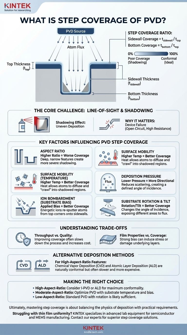
In the field of microfabrication, step coverage is a critical metric that defines the quality and uniformity of a thin film deposited over a non-flat surface. Specifically, it measures how well the deposited material conforms to the topography of the substrate, comparing the film's thickness on the sidewalls and bottom of a feature (like a trench or via) to its thickness on the top surface. Poor step coverage can lead to device failure, making it a central concern in semiconductor and MEMS manufacturing.
The core challenge of Physical Vapor Deposition (PVD) is its inherent line-of-sight nature, which naturally creates thin, non-uniform films in shadowed regions. Achieving good step coverage is therefore an exercise in overcoming this physical limitation by manipulating atomic mobility and flux directionality.
The Fundamental Challenge: Line-of-Sight Deposition
The physics of PVD are the root cause of step coverage issues. In PVD processes like sputtering or evaporation, atoms from a source target travel in straight lines through a vacuum to coat a substrate.
What is Step Coverage? A Formal Definition
Step coverage is expressed as a ratio. The most common definitions are the ratio of the film thickness on the vertical sidewall to the thickness on the top horizontal surface (t_sidewall / t_top) and the ratio of the thickness at the bottom of a feature to the thickness on top (t_bottom / t_top).
A perfect, or 100% conformal, coating would have a ratio of 1.0, meaning the film is equally thick everywhere. PVD rarely achieves this without significant process engineering.
The Geometric "Shadowing" Effect
Imagine trying to spray paint the inside of a tall, narrow box from above. The top edges will get a thick coat, the walls will receive very little paint, and the bottom may get none at all. This is the shadowing effect.
The source material in a PVD system acts like the spray paint. The opening of a trench or via "shadows" its own sidewalls and bottom from the incoming flux of atoms, resulting in a much thinner film in those areas.
Why Poor Step Coverage Leads to Failure
Inadequate step coverage in metal interconnects is a primary cause of device failure.
A thin or discontinuous film on the sidewall of a via creates an open circuit or a region of very high electrical resistance. This can prevent the device from functioning entirely or cause significant performance degradation and heat generation.
Key Factors Influencing PVD Step Coverage
Engineers have several levers to pull to improve step coverage. Each one aims to help depositing atoms find their way into the shadowed regions.
Aspect Ratio of the Feature
The aspect ratio (the ratio of a feature's height to its width) is the single most important geometric factor. High-aspect-ratio features, such as deep, narrow trenches, are exponentially more difficult to coat uniformly due to severe shadowing.
Surface Mobility (Temperature)
Heating the substrate during deposition gives the arriving atoms more thermal energy. This increased energy allows them to move, or diffuse, across the surface before locking into place.
This enhanced surface mobility enables atoms that land on the top surface to "crawl" over the edge and down the sidewall, significantly improving film uniformity.
Ion Bombardment (Substrate Bias)
Applying a negative voltage, or bias, to the substrate attracts positive ions from the plasma (like Argon in a sputter system). These energetic ions bombard the growing film.
This bombardment has two beneficial effects. It can physically knock atoms from the top corners of the feature, re-sputtering them onto the sidewalls. It also densifies the film as it grows.
Deposition Pressure
Lowering the process chamber pressure reduces the number of gas atoms between the source and the substrate. This means the depositing atoms are less likely to be scattered, leading to a more directional, line-of-sight flux.
While this may seem counterintuitive, a highly directional flux is a prerequisite for other advanced techniques, such as using collimators or ionized PVD, to work effectively.
Substrate Rotation and Tilt
A simple but effective mechanical solution is to rotate and tilt the substrate during deposition. This constantly changes the angle of incidence, allowing the source to "see" and deposit on different parts of the feature's sidewalls throughout the process.
Understanding the Trade-offs
Improving step coverage is not without cost and often involves balancing competing priorities.
Throughput vs. Quality
Techniques that improve step coverage, such as lowering the deposition rate or increasing substrate temperature, often increase the total process time. This reduces manufacturing throughput (wafers per hour) and increases cost.
Film Properties vs. Coverage
Applying a strong substrate bias can be very effective for coverage, but it can also induce compressive stress in the film or cause lattice damage to underlying layers. This can negatively impact the film's electrical or mechanical properties.
Alternative Deposition Methods
For the most demanding, high-aspect-ratio features, PVD may not be the right tool. Processes like Chemical Vapor Deposition (CVD) and Atomic Layer Deposition (ALD) are based on chemical reactions, not line-of-sight physics. They are naturally conformal and offer far superior step coverage, but typically at a higher cost and slower deposition rate.
Making the Right Choice for Your Goal
Selecting the right deposition strategy requires understanding your specific technical and economic constraints.
- If your primary focus is maximum conformality for critical, high-aspect-ratio features: You should investigate advanced techniques like Ionized PVD (I-PVD) or consider switching to a fundamentally more conformal method like ALD.
- If your primary focus is improving an existing PVD process for moderate-aspect-ratio features: Your best levers are increasing substrate temperature to enhance surface mobility and carefully applying a substrate bias to redirect flux.
- If your primary focus is cost-effective deposition on low-aspect-ratio features: A standard PVD process with substrate rotation is likely sufficient and provides the best balance of cost and performance.
Ultimately, mastering step coverage is about balancing the physics of deposition with the practical requirements of your device.
Summary Table:
| Factor | Impact on Step Coverage | Key Takeaway |
|---|---|---|
| Aspect Ratio | Higher ratio = worse coverage | Deep, narrow features are hardest to coat. |
| Surface Mobility (Temperature) | Higher temp = better coverage | Heating the substrate allows atoms to diffuse into shadowed areas. |
| Ion Bombardment (Bias) | Applied bias = better coverage | Energetic ions re-sputter atoms, improving sidewall deposition. |
| Deposition Pressure | Lower pressure = more directional flux | Creates a defined angle of incidence for advanced techniques. |
| Substrate Rotation/Tilt | Rotation/tilt = better coverage | Changes the deposition angle to coat different sidewalls. |
Struggling with thin film uniformity in your microfabrication process? KINTEK specializes in advanced lab equipment and consumables for semiconductor and MEMS manufacturing. Our expertise in PVD technologies can help you achieve superior step coverage and device reliability. Contact our experts today via our Contact Form to discuss your specific application and discover the right solution for your lab's needs.
Visual Guide
Related Products
- Chemical Vapor Deposition CVD Equipment System Chamber Slide PECVD Tube Furnace with Liquid Gasifier PECVD Machine
- RF PECVD System Radio Frequency Plasma-Enhanced Chemical Vapor Deposition RF PECVD
- Customer Made Versatile CVD Tube Furnace Chemical Vapor Deposition Chamber System Equipment
- Microwave Plasma Chemical Vapor Deposition MPCVD Machine System Reactor for Lab and Diamond Growth
- Custom CVD Diamond Coating for Lab Applications
People Also Ask
- What types of substrates are used in CVD to facilitate graphene films? Optimize Graphene Growth with the Right Catalyst
- How are carbon nanotubes grown? Master Scalable Production with Chemical Vapor Deposition
- Why is Chemical Vapor Deposition (CVD) equipment uniquely suited for constructing hierarchical superhydrophobic structures?
- How expensive is chemical vapor deposition? Understanding the True Cost of High-Performance Coating
- What happens during deposition chemistry? Building Thin Films from Gaseous Precursors


