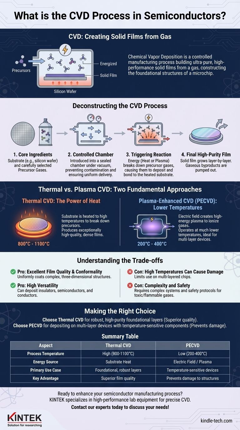
In essence, Chemical Vapor Deposition (CVD) is a highly controlled manufacturing process used in the semiconductor industry to build ultra-pure, high-performance solid films from a gas. Gaseous molecules, known as precursors, are introduced into a reaction chamber where they are energized and decompose. This chemical reaction causes a solid material to form and deposit layer-by-layer onto a heated substrate, such as a silicon wafer, creating the foundational structures of a microchip.
The core principle of CVD is not merely coating a surface, but rather constructing a new solid layer from chemical building blocks in a gas. The precise control over temperature, pressure, and gas chemistry is what enables the creation of the complex, high-purity materials essential for modern electronics.
Deconstructing the CVD Process
To truly understand CVD, it's best to visualize it as a sequence of controlled events, each with a specific purpose. The success of the entire process depends on the precise management of each stage.
The Core Ingredients: Substrate and Precursors
The process begins with two fundamental components. The first is the substrate, typically a silicon wafer, which serves as the foundation for the new layer.
The second is a carefully selected mixture of precursor gases. These gases contain the specific atoms (like silicon, carbon, or nitrogen) required to build the desired film. They are often mixed with inert carrier gases that help control the flow and reaction rate.
The Reaction Chamber: A Controlled Environment
The substrate and precursor gases are introduced into a sealed chamber under vacuum. This environment is critical for preventing contamination from unwanted particles or reactive gases like oxygen, which would introduce impurities into the film.
Precise control over the chamber's pressure and gas flow rates ensures that the precursor molecules are delivered to the substrate surface uniformly.
The Critical Step: Triggering the Chemical Reaction
This is the heart of the CVD process. Energy is introduced into the system to break apart the precursor gas molecules into highly reactive species (radicals, ions, or atoms).
These reactive species then diffuse toward the heated substrate. Upon contact with the hot surface, a series of chemical reactions occur, causing the desired solid material to deposit and bond to the substrate. The substrate itself can act as a catalyst, promoting the reaction directly on its surface.
The Final Product: A High-Purity Thin Film
As the reactions continue, a solid film grows on the substrate, one atomic layer at a time. Gaseous byproducts from the chemical reactions are continuously pumped out of the chamber as waste.
The result is an exceptionally pure and uniform thin film with specific electrical or physical properties tailored for its role in the semiconductor device.
Thermal vs. Plasma: The Two Fundamental Approaches
The method used to supply energy and trigger the chemical reaction is the primary distinction between different types of CVD. This choice has profound implications for the process and its applications.
Thermal CVD: The Power of Heat
In traditional Thermal CVD, the substrate is heated to very high temperatures (often 800°C to 1100°C). This intense thermal energy is what breaks down the precursor gases when they come into contact with the hot substrate surface.
This method is known for producing exceptionally high-quality and dense films. The high temperature provides the necessary activation energy for the chemical reactions to proceed efficiently.
Plasma-Enhanced CVD (PECVD): Lower Temperatures, Higher Reactivity
In Plasma-Enhanced CVD, an electric field (similar to how a microwave works) is used to ionize the gases, creating a plasma. This plasma is a highly energetic state of matter containing reactive ions and radicals.
Because the plasma itself energizes the gas molecules, the substrate does not need to be as hot. PECVD can operate at much lower temperatures (typically 200°C to 400°C), making it ideal for fabricating devices with structures that would be damaged by the extreme heat of Thermal CVD.
Understanding the Trade-offs
Like any engineering process, CVD involves balancing competing factors. Understanding these trade-offs is key to appreciating why a specific type of CVD is chosen for a particular application.
Pro: Excellent Film Quality and Conformality
CVD is renowned for producing films that are highly uniform and "conformal," meaning they can evenly coat complex, three-dimensional structures on a microchip. This is essential as device architectures become more intricate.
Pro: High Versatility
The process is incredibly versatile. By simply changing the precursor gases and process conditions, engineers can deposit a wide range of materials, including insulators (like silicon dioxide), semiconductors (like polysilicon), and conductors (like tungsten).
Con: High Temperatures Can Cause Damage
The primary drawback of Thermal CVD is its high temperature requirement. These temperatures can damage previously fabricated layers on a multi-layered chip, limiting its use to the early stages of manufacturing or on very robust materials.
Con: Complexity and Safety
CVD systems are complex and expensive. Furthermore, many precursor gases are highly toxic, flammable, or corrosive, demanding sophisticated safety protocols and handling systems.
Making the Right Choice for Your Goal
The decision to use a specific CVD process is dictated entirely by the requirements of the material being deposited and the thermal limitations of the device being built.
- If your primary focus is creating a robust, high-purity foundational layer: Thermal CVD is often the preferred method due to the superior film quality that results from its high-temperature process.
- If your primary focus is depositing a film on a multi-layer device with temperature-sensitive components: PECVD is the necessary choice, as its low-temperature plasma process avoids damaging the delicate structures already built on the wafer.
Ultimately, Chemical Vapor Deposition is a cornerstone technology, enabling the atomic-level construction that makes modern high-performance computing possible.
Summary Table:
| Aspect | Thermal CVD | Plasma-Enhanced CVD (PECVD) |
|---|---|---|
| Process Temperature | High (800°C - 1100°C) | Low (200°C - 400°C) |
| Energy Source | Substrate Heat | Electric Field / Plasma |
| Primary Use Case | Foundational, robust layers | Temperature-sensitive, multi-layer devices |
| Key Advantage | Superior film quality & density | Prevents damage to delicate structures |
Ready to enhance your semiconductor manufacturing process? KINTEK specializes in high-performance lab equipment and consumables for precise Chemical Vapor Deposition. Our solutions help you achieve the ultra-pure, uniform thin films essential for next-generation microchips. Contact our experts today to discuss how we can support your laboratory's specific CVD needs!
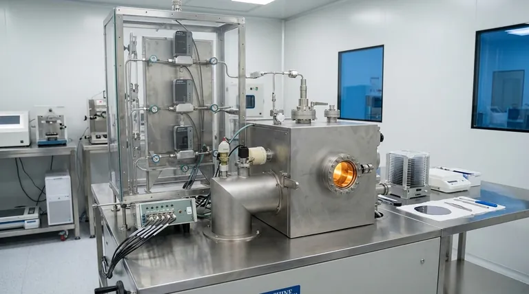
Visual Guide
Related Products
- Chemical Vapor Deposition CVD Equipment System Chamber Slide PECVD Tube Furnace with Liquid Gasifier PECVD Machine
- Customer Made Versatile CVD Tube Furnace Chemical Vapor Deposition Chamber System Equipment
- Microwave Plasma Chemical Vapor Deposition MPCVD Machine System Reactor for Lab and Diamond Growth
- 915MHz MPCVD Diamond Machine Microwave Plasma Chemical Vapor Deposition System Reactor
- Custom CVD Diamond Coating for Lab Applications
People Also Ask
- What is plasma enhanced chemical vapor deposition PECVD equipment? A Guide to Low-Temperature Thin Film Deposition
- How expensive is chemical vapor deposition? Understanding the True Cost of High-Performance Coating
- What happens during deposition chemistry? Building Thin Films from Gaseous Precursors
- How are carbon nanotubes grown? Master Scalable Production with Chemical Vapor Deposition
- Why is Chemical Vapor Deposition (CVD) equipment uniquely suited for constructing hierarchical superhydrophobic structures?


