At its core, DC (Direct Current) sputtering is a physical vapor deposition (PVD) technique used to create high-quality, thin films. In a vacuum chamber, a target made of the desired coating material is bombarded by energetic ions from a plasma. This physical impact ejects, or "sputters," atoms from the target, which then travel and deposit onto a substrate, forming a uniform coating.
DC sputtering is a highly effective and economical method for depositing thin films of metals and other electrically conductive materials. However, its reliance on a direct current makes it fundamentally unsuitable for insulating materials, which is its most significant limitation.
The Mechanics of DC Sputtering: From Plasma to Film
To understand DC sputtering, it's best to break it down into a sequence of events that transform a solid block of material into a precise, atomic-layer film.
Step 1: Creating the Vacuum Environment
First, a substrate (the object to be coated) and a target (the source material) are placed inside a sealed vacuum chamber. The air is pumped out, and the chamber is backfilled with a small, controlled amount of an inert gas, most commonly Argon.
This vacuum environment is critical, as it ensures the sputtered atoms can travel from the target to the substrate with minimal interference from other gas molecules.
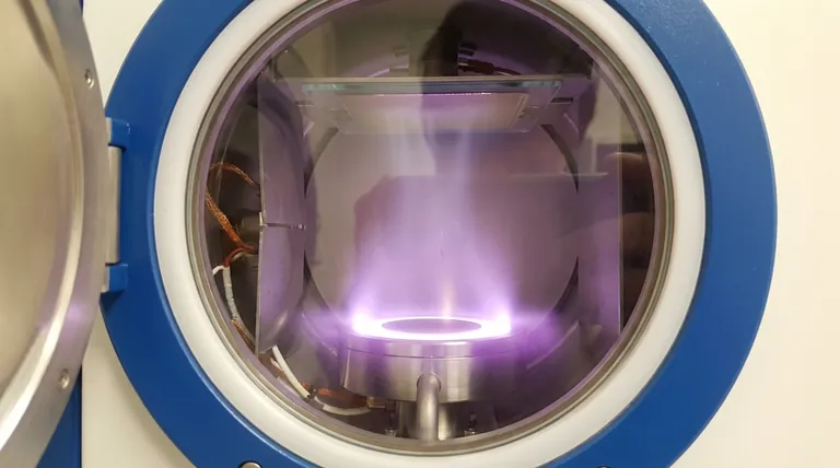
Step 2: Igniting the Plasma
A high-voltage Direct Current (DC) power source is applied, with the negative terminal connected to the target, making it a cathode. The chamber walls often serve as the anode.
This strong electric field energizes the free electrons in the chamber, causing them to collide with the neutral Argon atoms. These collisions knock electrons off the Argon atoms, creating positively charged Argon ions (Ar+) and more free electrons, resulting in a self-sustaining, glowing discharge known as a plasma.
Step 3: The Ion Bombardment
The positively charged Argon ions are now strongly attracted and accelerated toward the negatively charged target. They strike the target surface with significant kinetic energy.
Think of this process as a sandblaster operating at an atomic scale. The ions are the grit, and the target is the surface being eroded. Each impact transfers momentum, initiating a collision cascade within the target material.
Step 4: Deposition on the Substrate
When these collision cascades reach the target surface, they can eject individual atoms of the target material. These sputtered atoms travel through the vacuum chamber and land on the substrate.
As these atoms accumulate on the substrate surface, they nucleate and grow into a thin, dense, and highly adherent film. The process allows for precise control over the film's thickness and structure.
Understanding the Trade-offs and Limitations
While powerful, DC sputtering is not a universal solution. Its effectiveness is defined by a clear set of advantages and a critical, defining limitation.
The Conductive Material Requirement
The primary limitation of DC sputtering is its restriction to electrically conductive target materials, such as pure metals (Copper, Iron, Nickel) and some conductive alloys.
Because the target is powered by a DC source, it must be able to conduct electricity to maintain its negative charge and dissipate the charge brought by the impacting positive ions.
The Insulator Problem: Charge Build-up
If you attempt to use DC sputtering with an insulating material (like a ceramic or polymer), positive charge from the arriving Argon ions rapidly accumulates on the target surface. This build-up of positive charge neutralizes the negative potential of the target.
Eventually, the target is no longer "negative," and it ceases to attract the positive Argon ions. The plasma collapses, and the sputtering process stops completely. This phenomenon is known as a "disappearing anode" and makes standard DC sputtering unworkable for non-conductive materials.
High Deposition Rates and Scalability
For its intended use with metals, DC sputtering is highly efficient. It offers relatively high deposition rates and is a cost-effective, reliable, and scalable process for coating large areas, making it a workhorse in many industrial applications.
Is DC Sputtering the Right Choice for Your Application?
Choosing a deposition technique requires matching the process capabilities with your material and end goal.
- If your primary focus is depositing pure metals or conductive alloys: DC sputtering is an excellent, cost-effective, and highly reliable choice for creating dense, high-purity films.
- If your primary focus is depositing insulating materials (like oxides or nitrides): DC sputtering is unsuitable. You must use an alternative like RF (Radio Frequency) sputtering, which uses an AC field to avoid charge build-up on the target.
- If your primary focus is high-volume, large-area coating with a conductive material: The simplicity and efficiency of DC sputtering make it a leading candidate for industrial-scale production.
Understanding the fundamental role of electrical conductivity is the key to leveraging the power of DC sputtering effectively.
Summary Table:
| Feature | Description |
|---|---|
| Process | Physical Vapor Deposition (PVD) using a DC power supply. |
| Best For | Depositing thin films of conductive materials (metals, alloys). |
| Key Limitation | Cannot be used with insulating materials due to charge build-up. |
| Primary Advantage | High deposition rates, cost-effective, and scalable for large areas. |
Need a reliable solution for depositing high-quality metal thin films?
KINTEK specializes in lab equipment and consumables, providing robust DC sputtering systems ideal for your conductive material coating needs. Our expertise ensures you get a scalable, cost-effective solution for dense, high-purity films.
Contact our experts today to discuss how our DC sputtering technology can enhance your laboratory's capabilities!
Visual Guide

Related Products
- Spark Plasma Sintering Furnace SPS Furnace
- Multi Heating Zones CVD Tube Furnace Machine Chemical Vapor Deposition Chamber System Equipment
- Vacuum Induction Melting Spinning System Arc Melting Furnace
- Circulating Water Vacuum Pump for Laboratory and Industrial Use
People Also Ask
- What is the difference between spark plasma sintering and flash sintering? A Guide to Advanced Sintering Methods
- Why are Spark Plasma Sintering (SPS) furnaces or hot presses utilized in the preparation of Li3PS4 solid electrolytes?
- What is SPS sintering method? A Guide to High-Speed, High-Performance Material Fabrication
- What is the theory of spark plasma sintering? A Guide to Rapid, Low-Temperature Densification
- What is the pressure for spark plasma sintering? A Guide to Optimizing SPS Parameters


