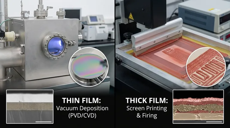
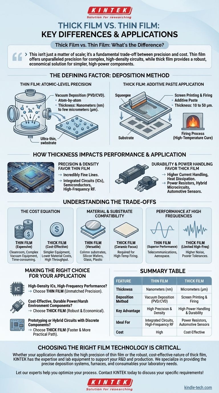
At its core, the difference between thick film and thin film technology comes down to two key factors: the deposition method and the resulting material thickness. Thin films are built atom-by-atom in a vacuum, resulting in layers measured in nanometers. Thick films are applied as a paste using a screen-printing process, creating much thicker layers measured in micrometers.
This isn't just a matter of scale; it's a fundamental trade-off between precision and cost. Thin film offers unparalleled precision for complex, high-density circuits, while thick film provides a robust, economical solution for simpler, high-power components.
The Defining Factor: Deposition Method
The "thick" vs. "thin" distinction originates entirely from how the material is applied to the substrate. This process dictates every subsequent characteristic of the technology.
Thin Film: Atomic-Level Precision
Thin film deposition occurs in a vacuum chamber. Processes like Physical Vapor Deposition (PVD) (e.g., sputtering) or Chemical Vapor Deposition (CVD) are used.
These methods deposit material one molecule or atom at a time, creating an extremely uniform and pure layer. The resulting film thickness is typically between a few nanometers (nm) and a few micrometers (µm).
Thick Film: Additive Paste Application
Thick film technology is an additive process, most commonly screen printing. It functions much like stenciling.
A specialized paste—containing conductive, resistive, or dielectric particles—is pushed through a patterned screen onto a substrate, usually ceramic. The part is then fired in a high-temperature furnace to cure the paste, binding it to the substrate. This creates layers that are typically 10 to 50 µm thick.
How Thickness Impacts Performance and Application
The manufacturing process and resulting thickness directly influence what each technology excels at.
Precision and Density Favor Thin Film
The atomic-level control of thin film deposition allows for incredibly fine lines and tight tolerances. This is what enables the creation of modern microelectronics.
This precision is essential for integrated circuits (ICs), semiconductors, and high-frequency RF components where even minute variations can impact performance.
Durability and Power Handling Favor Thick Film
The greater volume of material in thick film layers makes them inherently more robust. They can handle higher currents and dissipate more heat.
This makes thick film ideal for power resistors, hybrid microcircuits, and automotive sensors that must withstand significant thermal and physical stress.
Understanding the Trade-offs
Choosing between these technologies requires a clear understanding of their inherent limitations and benefits.
The Cost Equation
Thin film is expensive. It requires a cleanroom environment, complex vacuum equipment, and a time-consuming deposition process.
Thick film is significantly more cost-effective. The equipment is simpler, material costs are lower, and the manufacturing throughput is much higher, making it ideal for mass production of simpler components.
Material and Substrate Compatibility
Thin film processes are versatile and can be used on a wide range of substrates, including silicon wafers, glass, and plastics.
Thick film is almost always applied to ceramic substrates (like alumina) because they can withstand the high temperatures required for the firing process.
Performance at High Frequencies
Thin film's precise geometric definition and purer materials result in superior performance for high-frequency applications, such as those in telecommunications and aerospace.
Thick film resistors and conductors tend to have higher noise and poorer tolerances, which can limit their use in sensitive, high-frequency designs.
Making the Right Choice for Your Application
The correct technology is the one that best aligns with your project's balance of performance, durability, and budget.
- If your primary focus is high-density integrated circuits or high-frequency performance: Thin film is the only viable choice due to its unmatched precision.
- If your primary focus is cost-effective, durable components for power applications or harsh environments: Thick film offers a robust and economical solution.
- If you are prototyping or producing hybrid circuits with discrete components: Thick film's simpler process often provides a faster and more practical path.
Ultimately, understanding these fundamental differences empowers you to select the technology that aligns perfectly with your engineering and business goals.
Summary Table:
| Feature | Thin Film | Thick Film |
|---|---|---|
| Thickness | Nanometers (nm) | Micrometers (µm) |
| Deposition Method | Vacuum Deposition (PVD/CVD) | Screen Printing & Firing |
| Key Advantage | High Precision & Density | High Power Handling & Durability |
| Ideal For | Integrated Circuits, High-Frequency RF | Power Resistors, Automotive Sensors |
| Cost | High | Cost-Effective |
Choosing the right film technology is critical for your project's success. Whether your application demands the high precision of thin film or the robust, cost-effective nature of thick film, KINTEK has the expertise and lab equipment to support your R&D and production.
We specialize in providing the precise deposition systems, furnaces, and consumables your laboratory needs. Let our experts help you optimize your process. Contact KINTEK today to discuss your specific requirements!
Visual Guide
Related Products
- Aluminum-Plastic Flexible Packaging Film for Lithium Battery Packaging
- Battery Lab Equipment 304 Stainless Steel Strip Foil 20um Thick for Battery Test
- Lab Blown Film Extrusion Three Layer Co-Extrusion Film Blowing Machine
- Lab Plastic PVC Calender Stretch Film Casting Machine for Film Testing
- Custom CVD Diamond Coating for Lab Applications
People Also Ask
- How is aluminum foil utilized as a consumable during the assembly of cold sintering molds? Optimize Tooling Longevity
- How to check if a lithium battery is good? Safely Test Voltage, Capacity & Internal Resistance
- What are the three types of lamination? Choose the Perfect Finish for Your Print Project
- What is the difference between single layer film and multi layer film? A Guide to Material Selection
- How to tell if a lithium-ion battery is bad? Spot the critical signs of failure before it's too late.


