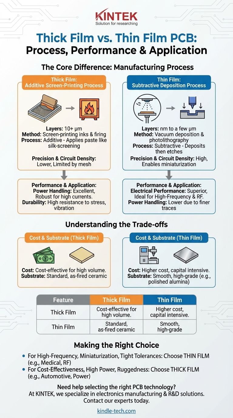
The fundamental difference between thick film and thin film technology lies in the manufacturing process used to deposit materials onto a substrate. Thick film technology uses a screen-printing method to apply a paste, resulting in layers typically 10 microns (µm) or thicker. In contrast, thin film technology uses vacuum deposition or sputtering techniques to create much finer layers, usually in the range of nanometers (nm) to a few microns.
The choice is a classic engineering trade-off: Thick film offers a robust, cost-effective solution for high-power and general-purpose applications, while thin film provides superior precision and performance for high-frequency, high-density circuits where miniaturization is critical.
The Core Difference: Manufacturing Process
The manufacturing method is the source of all subsequent differences in performance, cost, and application.
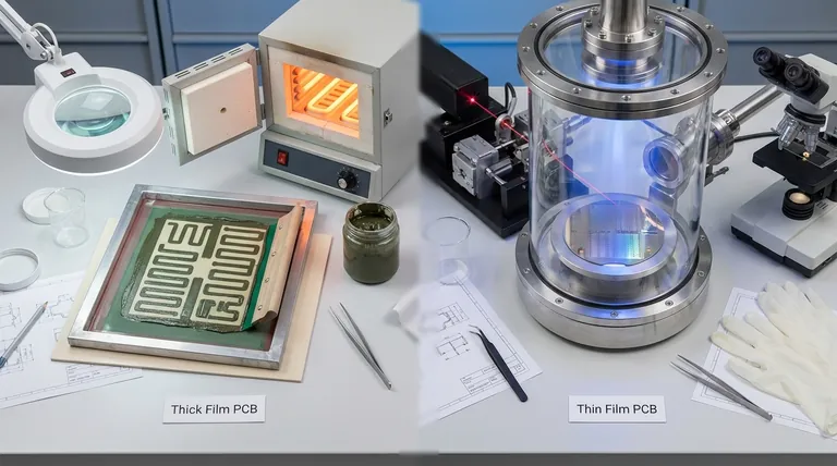
Thick Film: An Additive Screen-Printing Process
Thick film circuits are created by printing special pastes, known as "inks," onto a ceramic substrate like alumina. This process is analogous to silk-screening a T-shirt.
A mesh screen with a stenciled circuit pattern is used to squeegee the paste onto the substrate. The substrate is then fired in a high-temperature furnace to fuse the paste, creating durable conductive, resistive, or dielectric layers.
Thin Film: A Subtractive Deposition Process
Thin film manufacturing is a more precise, multi-step process conducted in a vacuum. A layer of material is first deposited evenly across the entire substrate using methods like sputtering or vapor deposition.
Next, a photolithography process is used to selectively remove material, etching away the unwanted portions to leave behind the desired circuit pattern. This is a subtractive method that allows for extremely fine lines and tight tolerances.
How Process Dictates Performance and Application
The contrast in manufacturing directly impacts the final circuit's capabilities.
Precision and Circuit Density
Thin film is the clear winner for precision. The photolithographic etching process enables the creation of much finer lines and spaces, allowing for higher component density and overall circuit miniaturization.
Thick film's screen-printing process is inherently less precise. The mesh of the screen and the viscosity of the paste limit the minimum feature size, making it unsuitable for highly compact designs.
Electrical Performance and Frequency
For high-frequency applications (RF, microwave), thin film is superior. Its uniform, pure, and precisely defined conductive layers result in excellent signal integrity, low noise, and predictable performance.
Thick film conductors and resistors are less uniform, which can introduce parasitic capacitance and inductance. This makes them less ideal for signals where precise impedance control is critical.
Power Handling and Durability
Thick film excels in power applications. The thicker cross-sectional area of its printed conductors can handle significantly higher currents and dissipate more heat than thin film traces.
The fired-on nature of thick film pastes also creates an exceptionally durable circuit that is highly resistant to mechanical stress, vibration, and thermal shock.
Understanding the Trade-offs: Cost vs. Precision
Your choice will almost always involve balancing budget against performance requirements.
The Cost Equation
Thick film is generally more cost-effective, particularly for high-volume production. The screen-printing equipment and materials are less expensive, and the process is faster with higher throughput.
Thin film manufacturing requires a significant capital investment in vacuum chambers and cleanroom facilities. The process is more complex and time-consuming, leading to a higher cost per unit, especially for tooling and setup.
Substrate and Material Demands
Thin film processes demand very smooth substrates, such as polished alumina or quartz, to ensure the uniformity of the deposited layers. These high-grade materials add to the overall cost.
Thick film is more forgiving and works well on standard, as-fired ceramic substrates, which are less expensive and more readily available.
Making the Right Choice for Your Application
Use your primary goal to guide your decision between these two robust technologies.
- If your primary focus is high-frequency performance, miniaturization, or tight tolerances: Choose thin film for its superior precision, ideal for medical implants, optical networking components, and RF/microwave modules.
- If your primary focus is cost-effectiveness, high power handling, or ruggedness: Choose thick film for its robust nature and lower manufacturing cost, making it perfect for automotive sensors, industrial controls, and power electronics.
By understanding how the manufacturing process dictates performance, you can confidently select the technology that aligns perfectly with your project's technical and budgetary goals.
Summary Table:
| Feature | Thick Film PCB | Thin Film PCB |
|---|---|---|
| Layer Thickness | 10+ microns (µm) | Nanometers (nm) to a few microns |
| Manufacturing Process | Screen-printing & firing | Vacuum deposition & photolithography |
| Precision & Density | Lower, limited by screen mesh | High, enables miniaturization |
| Electrical Performance | Good for power, less ideal for high-frequency | Superior for high-frequency & RF |
| Power Handling | Excellent, robust for high currents | Lower due to finer traces |
| Cost | Cost-effective, ideal for high-volume | Higher cost, specialized equipment |
| Ideal Applications | Automotive sensors, power electronics, industrial controls | Medical implants, RF/microwave modules, optical networking |
Need help selecting the right PCB technology for your project?
At KINTEK, we specialize in providing high-quality lab equipment and consumables for electronics manufacturing and R&D. Whether you're developing thick film circuits for rugged applications or thin film components requiring precision, our expertise and products can support your success.
Contact our experts today to discuss your specific requirements and discover how KINTEK can enhance your laboratory's capabilities.
Visual Guide
Related Products
- Aluminum-Plastic Flexible Packaging Film for Lithium Battery Packaging
- Electron Beam Evaporation Coating Oxygen-Free Copper Crucible and Evaporation Boat
- Copper Foam
- Thin-Layer Spectral Electrolysis Electrochemical Cell
- Silicon Carbide (SIC) Ceramic Plate for Engineering Advanced Fine Ceramics
People Also Ask
- What is the difference between monolayer and multilayer film? Choose the Right Packaging for Your Product
- What is organic thin film? A Guide to Engineered Molecular Layers for Advanced Tech
- What is the thinnest coating? Unlocking Unique Properties at the Atomic Scale
- What are the properties of Aluminium (Al) relevant to its use in coatings? High Reflectivity & Conductivity Explored
- Is there a way to test lithium batteries? Understand Voltage vs. True Health