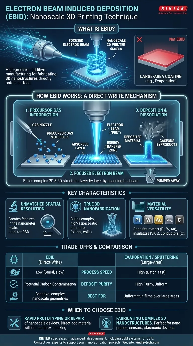
In short, Electron Beam Induced Deposition (EBID) is a high-precision additive manufacturing technique used to fabricate three-dimensional nanostructures directly onto a surface. It functions like a nanoscale 3D printer, using a finely focused electron beam to "draw" structures by decomposing a precursor gas. This is fundamentally different from the more common large-area coating method known as Electron Beam Evaporation, which vaporizes a solid material to blanket an entire surface.
The critical distinction is that EBID 'draws' structures by decomposing a precursor gas with a focused electron beam, while Electron Beam Evaporation blankets a surface by vaporizing a solid material. EBID offers unparalleled precision for prototyping and fabrication at the nanoscale.
How EBID Works: A Direct-Write Mechanism
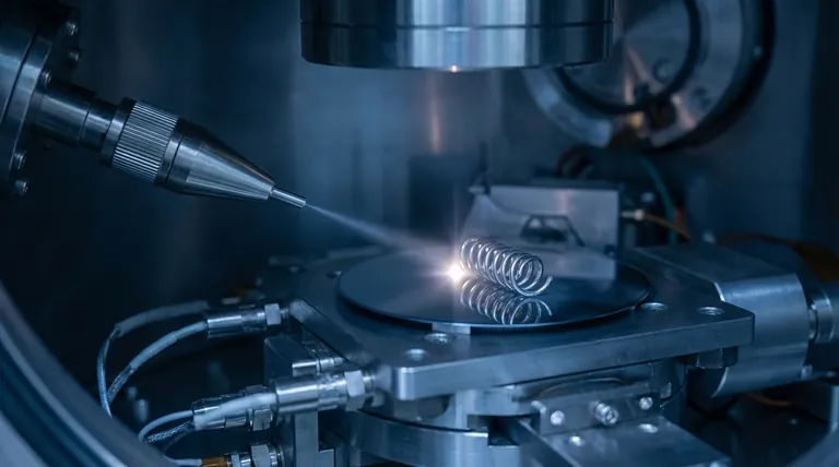
The EBID process is typically performed inside the vacuum chamber of a Scanning Electron Microscope (SEM) or a similar electron beam instrument. This allows for simultaneous imaging and fabrication.
The Precursor Gas Introduction
A chemical precursor, usually an organometallic compound in a gaseous state, is introduced into the high-vacuum chamber. This gas is delivered through a fine needle positioned very close to the substrate surface.
The gas molecules spread out and temporarily adsorb (stick) to the substrate, forming a thin, mobile layer.
The Focused Electron Beam
A highly focused beam of electrons, controlled with precision by the microscope's electronics, is directed at a specific point on the substrate. This beam serves as the "pen" for the deposition process.
The Deposition Mechanism
When the electron beam interacts with the adsorbed precursor gas molecules, it transfers energy. This energy breaks the chemical bonds within the molecules.
This process, known as dissociation, splits the molecule into volatile (gaseous) and non-volatile (solid) components. The volatile parts are pumped away by the vacuum system, while the solid, non-volatile material remains deposited on the substrate precisely where the beam was focused.
By scanning the beam across the surface, complex 2D and 3D structures can be built up layer-by-layer.
Key Characteristics of EBID
Understanding EBID's core attributes is essential to knowing when it is the right tool for a specific task.
Unmatched Spatial Resolution
Because the process is driven by a finely focused electron beam, EBID can create features with dimensions well into the nanometer scale. This makes it a powerful tool for nanotechnology research and development.
True 3D Nanofabrication
Unlike many lithographic techniques which are planar, EBID is an additive, direct-write process. It can be used to build complex, three-dimensional structures with high aspect ratios, such as pillars, wires, and coils.
Material Versatility
The properties of the deposited material are determined by the precursor gas used. A wide variety of materials can be deposited, including metals like platinum, tungsten, and gold, as well as insulators like silicon dioxide and conductors like carbon.
Understanding the Trade-offs and Limitations
While powerful, EBID is not a universal solution. Its unique characteristics come with significant trade-offs compared to other deposition methods.
Process Speed and Throughput
EBID is an inherently slow, serial process. It builds structures one point at a time, making it unsuitable for high-volume manufacturing or coating large areas. Techniques like the Electron Beam Evaporation described in the references are vastly faster for batch processing.
Purity of the Deposit
A common challenge with EBID is the purity of the deposited material. The precursor molecules often contain carbon, and incomplete dissociation can lead to significant carbon co-deposition. This can negatively impact the electrical or mechanical properties of the final nanostructure.
Comparison to Other Techniques
Compared to Electron Beam Evaporation or Sputtering, EBID is a low-throughput, high-precision technique. Those methods are ideal for creating uniform, high-purity thin films over large areas, whereas EBID excels at creating bespoke, complex geometries on a very small scale.
When to Choose EBID for Your Application
Selecting the right fabrication method depends entirely on your end goal.
- If your primary focus is rapid prototyping or repair of nanoscale devices: EBID is an ideal choice for its direct-write capability, allowing you to add material precisely where it's needed without complex masking steps.
- If your primary focus is fabricating complex 3D nanostructures: EBID provides a level of additive control that is difficult to achieve with other methods, making it perfect for creating nano-probes, sensors, or plasmonic devices.
- If your primary focus is creating high-purity, uniform thin films over large areas: You should consider techniques like Electron Beam Evaporation or Magnetron Sputtering, which are designed for high-throughput and excellent film quality.
Ultimately, EBID is a specialized tool that provides unmatched control for creating custom structures at the smallest scales.
Summary Table:
| Aspect | EBID Characteristic |
|---|---|
| Process Type | Additive, direct-write |
| Best For | Prototyping, custom 3D nanostructures |
| Resolution | Nanometer scale |
| Throughput | Low (serial process) |
| Key Advantage | Unmatched 3D control and geometry complexity |
| Common Limitation | Potential for carbon contamination in deposits |
Need to create custom nanostructures or prototype nanoscale devices?
KINTEK specializes in providing the advanced lab equipment, including SEM systems and related technologies, that enable cutting-edge techniques like Electron Beam Induced Deposition. Our expertise can help you select the right tools for your specific R&D or fabrication goals in nanotechnology.
Contact our experts today to discuss how we can support your nanofabrication projects with precision equipment and consumables.
Visual Guide
Related Products
- Electron Beam Evaporation Coating Oxygen-Free Copper Crucible and Evaporation Boat
- RF PECVD System Radio Frequency Plasma-Enhanced Chemical Vapor Deposition RF PECVD
- Chemical Vapor Deposition CVD Equipment System Chamber Slide PECVD Tube Furnace with Liquid Gasifier PECVD Machine
- HFCVD Machine System Equipment for Drawing Die Nano-Diamond Coating
- 915MHz MPCVD Diamond Machine Microwave Plasma Chemical Vapor Deposition System Reactor
People Also Ask
- What are the applications of electron beams? From Nanoscale Imaging to Industrial Manufacturing
- What is the deposition rate of e-beam evaporation? Control Thin Film Quality and Speed
- What is e-beam evaporation? Achieve High-Purity Thin Film Deposition for Your Lab
- What are the applications of e-beam evaporation? Achieve High-Purity Coatings for Optics & Electronics
- What is the container that holds the metal source material called in e-beam evaporation? Ensure Purity and Quality in Your Thin-Film Deposition


