In essence, the function of film deposition is to strategically apply a micro-thin coating onto a material's surface to give it new properties. This process enhances a base material, known as a substrate, making it suitable for a specific application. These enhancements can range from protecting a component against scratches and extreme heat to fundamentally changing its electrical conductivity or how it interacts with light.
The core purpose of film deposition is not merely to coat an object, but to engineer its surface. It allows us to combine the bulk properties of one material (like the strength of steel) with the desired surface properties of another (like the wear-resistance of a ceramic), creating a composite material optimized for a specific task.
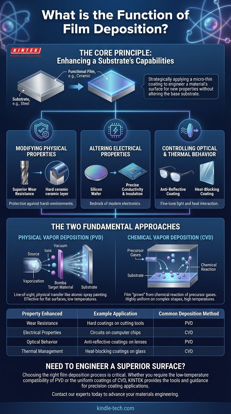
The Core Principle: Enhancing a Substrate's Capabilities
Film deposition works from a simple premise: a material that is ideal for its structural purpose may lack the necessary surface characteristics. Deposition solves this by adding a thin, functional layer without altering the underlying substrate.
Modifying Physical and Mechanical Properties
Many applications require surfaces that can withstand harsh physical environments. A deposited film can provide this protection.
For example, a thin layer of a hard ceramic compound can be deposited onto a metal cutting tool. This grants the tool superior wear resistance and a longer operational life than the metal alone could provide.
Altering Electrical Properties
Film deposition is the bedrock of the modern electronics industry. It allows for the precise creation of conductive, insulating, and semi-conductive layers.
By depositing specific metallic or oxide films in intricate patterns, we create the microscopic circuits found in computer chips. This process transforms a non-conductive silicon wafer into a complex electronic device.
Controlling Optical and Thermal Behavior
The interaction of a material with light and heat can be finely tuned using deposited films.
An anti-reflective coating on eyeglasses is a classic example. This deposited film is engineered to manipulate light waves, reducing glare. Similarly, coatings on architectural glass can block infrared radiation, keeping buildings cooler without reducing visible light.
The Two Fundamental Approaches
Deposition processes are typically categorized by how they transport the coating material to the substrate surface within a vacuum chamber. The two primary methods are Physical Vapor Deposition (PVD) and Chemical Vapor Deposition (CVD).
Physical Vapor Deposition (PVD)
PVD is a "line-of-sight" process that physically transfers material onto the substrate. Think of it as a highly controlled form of spray painting at the atomic level.
The source material is vaporized through methods like heating or sputtering (bombarding it with ions). This vapor then travels through the vacuum and condenses onto the cooler substrate, forming the film.
Chemical Vapor Deposition (CVD)
CVD is a chemical process where the film is "grown" directly on the substrate from precursor gases. This is more analogous to dew forming on a cool surface.
One or more volatile precursor gases are introduced into the chamber, which then react or decompose on the substrate's surface to produce the desired solid film.
Understanding the Trade-offs
Neither PVD nor CVD is universally superior; the choice depends entirely on the application, the substrate material, and the desired film properties. Understanding their limitations is key to making an informed decision.
Process Temperature and Substrate Compatibility
CVD processes often require very high temperatures to initiate the necessary chemical reactions. This can damage or warp heat-sensitive substrates like plastics or certain alloys.
PVD, in contrast, can generally be performed at much lower temperatures, making it compatible with a wider range of materials.
Film Uniformity and Coverage
Because CVD involves a gas that fills the entire chamber, it excels at producing highly uniform (conformal) coatings, even on complex shapes with internal surfaces and crevices.
PVD's line-of-sight nature means it is most effective on flatter surfaces. It can struggle to evenly coat intricate geometries, leading to thinner or non-existent coverage in "shadowed" areas.
Making the Right Choice for Your Application
Selecting the correct deposition method requires aligning the process capabilities with your primary goal.
- If your primary focus is wear resistance or optical coatings on relatively simple shapes: PVD is often the more direct, cost-effective, and lower-temperature solution.
- If your primary focus is creating a highly uniform, pure film inside complex geometries: CVD's ability to "grow" a conformal layer makes it the superior choice, provided the substrate can handle the heat.
- If your primary focus is coating heat-sensitive materials like polymers or electronics: A low-temperature PVD process is almost always the necessary path.
Ultimately, film deposition empowers us to create materials that are more than the sum of their parts, enabling the high-performance technology that defines our world.
Summary Table:
| Property Enhanced | Example Application | Common Deposition Method |
|---|---|---|
| Wear Resistance | Hard coatings on cutting tools | PVD (Physical Vapor Deposition) |
| Electrical Properties | Circuits on computer chips | CVD (Chemical Vapor Deposition) |
| Optical Behavior | Anti-reflective coatings on lenses | PVD (Physical Vapor Deposition) |
| Thermal Management | Heat-blocking coatings on glass | CVD (Chemical Vapor Deposition) |
Need to Engineer a Superior Surface?
Choosing the right film deposition process is critical for achieving the specific surface properties your application demands. Whether you require the low-temperature compatibility of PVD for sensitive substrates or the highly uniform coatings of CVD for complex geometries, KINTEK has the expertise and equipment to support your project.
As a specialist in laboratory equipment and consumables, we provide the tools and guidance necessary for precision coating applications. Let us help you select the ideal deposition solution to enhance your material's performance and durability.
Contact our experts today to discuss your specific requirements and discover how KINTEK can advance your materials engineering capabilities.
Visual Guide
Related Products
- Aluminized Ceramic Evaporation Boat for Thin Film Deposition
- Tungsten Evaporation Boat for Thin Film Deposition
- Hemispherical Bottom Tungsten Molybdenum Evaporation Boat
- Electron Beam Evaporation Coating Oxygen-Free Copper Crucible and Evaporation Boat
- Custom CVD Diamond Coating for Lab Applications
People Also Ask
- What is the chemical method for thin film deposition? Build Films from the Molecular Level Up
- What are the alternatives to sputtering? Choose the Right Thin Film Deposition Method
- What is the source of evaporation for thin film? Choosing Between Thermal and E-Beam Methods
- What are thin films deposited by evaporation? A Guide to High-Purity Coating
- What is thin film deposition? Unlock Advanced Surface Engineering for Your Materials


