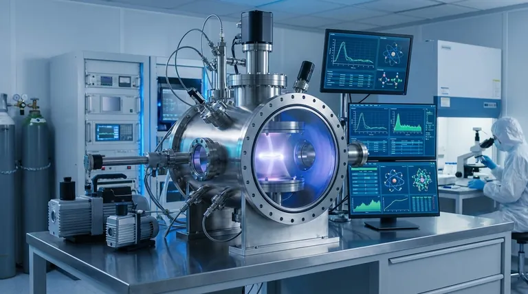
For depositing extremely controlled thin films, the definitive method is Atomic Layer Deposition (ALD). This chemical deposition technique operates by exposing a substrate to sequential, self-limiting chemical reactions, allowing for the growth of a film one atomic layer at a time. This process provides unparalleled precision over film thickness, composition, and uniformity, far surpassing most other common methods.
The core challenge in thin film deposition is balancing precision with speed and cost. While many techniques can produce thin films, only methods like Atomic Layer Deposition (ALD) offer true atomic-level control, which is essential for manufacturing modern high-performance electronics and advanced optical components.
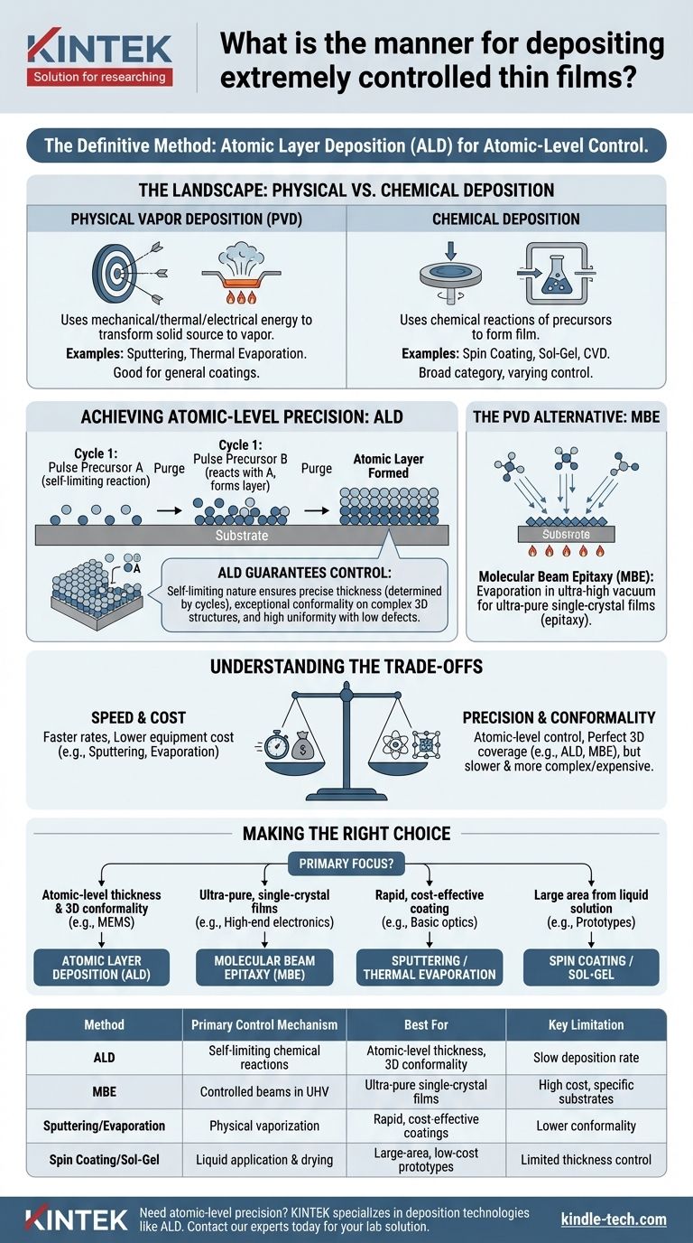
The Landscape: Physical vs. Chemical Deposition
To understand why ALD provides such high control, it is essential to first distinguish between the two primary categories of deposition techniques. Each category operates on a different fundamental principle.
Physical Vapor Deposition (PVD)
PVD methods use mechanical, thermal, or electrical energy to transform a solid source material into a vapor, which then condenses onto a substrate.
Common PVD techniques include thermal evaporation, where the source material is heated until it vaporizes, and sputtering, where a target is bombarded with high-energy ions (like argon plasma) to eject atoms that then coat the substrate. These are workhorse methods for many industries.
Chemical Deposition
Chemical methods use chemical reactions to form the film on the substrate surface. The source materials, known as precursors, are often liquids or gases that react or decompose to create the desired solid film.
This category is broad, including methods like spin coating, sol-gel, and Chemical Vapor Deposition (CVD). CVD is a widely used technique where precursor gases react in a chamber to deposit a film, but its control is generally not at the atomic-layer level.
Achieving Atomic-Level Precision
For applications demanding the highest possible control over thickness and uniformity, specialized techniques are required. ALD is the leading method in this domain.
The Principle of Atomic Layer Deposition (ALD)
ALD is a subtype of chemical vapor deposition, but with a crucial difference. Instead of introducing all precursor chemicals at once, ALD uses a sequential, pulsed process.
Each cycle consists of two or more self-limiting steps. A pulse of the first precursor is introduced, which reacts with the substrate surface until all available reaction sites are occupied. The excess precursor is then purged. Next, a pulse of the second precursor is introduced to react with the first layer, completing the film's single atomic layer.
How ALD Guarantees Control
The power of ALD lies in its self-limiting nature. The reactions automatically stop after one full atomic layer is formed in each cycle. This means film thickness is simply determined by the number of deposition cycles performed.
This process ensures exceptional conformality (the ability to coat complex, three-dimensional structures uniformly) and repeatability over very large areas, with extremely low defect density.
The PVD Alternative: Molecular Beam Epitaxy (MBE)
In the physical deposition world, Molecular Beam Epitaxy (MBE) is the counterpart to ALD for high-precision applications. MBE involves the evaporation of elemental sources in an ultra-high vacuum environment.
MBE "sprays" beams of atoms or molecules onto a heated crystalline substrate with extreme precision. It is particularly valued for creating very high-purity single-crystal films (epitaxy), which are critical for high-end semiconductors and research.
Understanding the Trade-offs
Extreme precision does not come without compromises. Choosing a deposition method requires balancing technical requirements with practical constraints.
Speed vs. Perfection
The primary drawback of ALD is its slow deposition rate. Because films are built one atomic layer at a time, the process is inherently much slower than techniques like sputtering or evaporation, which deposit material continuously.
Cost and Complexity
Systems for ALD and MBE are significantly more complex and expensive than standard PVD or wet chemical setups. The precursor chemicals used in ALD can also be costly and require specialized handling.
Material and Substrate Limitations
While versatile, ALD is dependent on the availability of suitable precursor chemicals that exhibit self-limiting reaction behavior. Similarly, MBE is best suited for creating crystalline films on specific types of crystalline substrates.
Making the Right Choice for Your Application
Selecting the correct deposition method depends entirely on the required level of control and the end-use of the component.
- If your primary focus is atomic-level thickness control and perfect uniformity over complex shapes (e.g., semiconductor gates, MEMS): Atomic Layer Deposition (ALD) is the superior choice.
- If your primary focus is creating ultra-pure, single-crystal films for high-performance electronics or research: Molecular Beam Epitaxy (MBE) is a leading PVD alternative.
- If your primary focus is rapid, cost-effective coating for general applications (e.g., protective layers, basic optics): Sputtering or thermal evaporation are standard, reliable workhorses.
- If your primary focus is depositing from a liquid solution for large areas at low cost (e.g., some solar cells, lab prototypes): Techniques like spin coating or sol-gel offer a practical solution.
Ultimately, the right technique is the one that meets your specific tolerance for film thickness, uniformity, and purity without exceeding your project's budget and time constraints.
Summary Table:
| Method | Primary Control Mechanism | Best For | Key Limitation |
|---|---|---|---|
| Atomic Layer Deposition (ALD) | Self-limiting chemical reactions | Atomic-level thickness, 3D conformality | Slow deposition rate |
| Molecular Beam Epitaxy (MBE) | Controlled atomic/molecular beams in ultra-high vacuum | Ultra-pure single-crystal films | High cost, specific substrates |
| Sputtering / Thermal Evaporation | Physical vaporization of a target | Rapid, cost-effective coatings | Lower conformality on complex shapes |
| Spin Coating / Sol-Gel | Liquid precursor application & drying | Large-area, low-cost prototypes from solution | Limited thickness control & uniformity |
Need to deposit films with atomic-level precision? KINTEK specializes in lab equipment and consumables, serving advanced laboratory needs. Our expertise in deposition technologies like ALD can help you achieve the exact film properties your research or production requires. Contact our experts today to discuss your specific application and find the perfect solution for your lab!
Visual Guide
Related Products
- Chemical Vapor Deposition CVD Equipment System Chamber Slide PECVD Tube Furnace with Liquid Gasifier PECVD Machine
- RF PECVD System Radio Frequency Plasma-Enhanced Chemical Vapor Deposition RF PECVD
- HFCVD Machine System Equipment for Drawing Die Nano-Diamond Coating
- Customer Made Versatile CVD Tube Furnace Chemical Vapor Deposition Chamber System Equipment
- 915MHz MPCVD Diamond Machine Microwave Plasma Chemical Vapor Deposition System Reactor
People Also Ask
- What happens during deposition chemistry? Building Thin Films from Gaseous Precursors
- What are the processes of vapor phase deposition? Understand CVD vs. PVD for Superior Thin Films
- What is the chemical vapor deposition growth process? Build Superior Thin Films from the Atom Up
- What types of substrates are used in CVD to facilitate graphene films? Optimize Graphene Growth with the Right Catalyst
- How are carbon nanotubes grown? Master Scalable Production with Chemical Vapor Deposition


