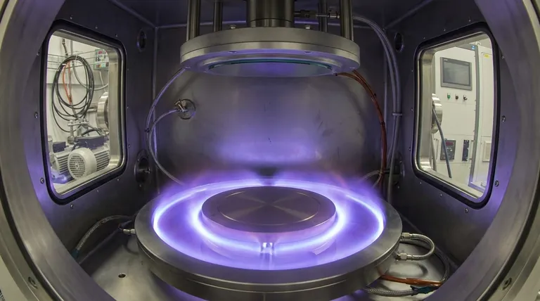
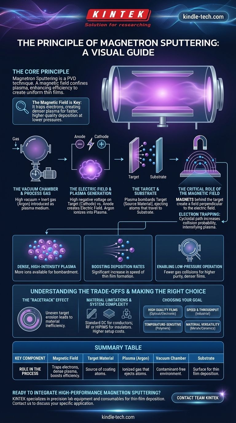
At its core, the principle of magnetron sputtering is a physical vapor deposition (PVD) technique that uses a magnetic field to enhance the efficiency of creating a thin film. In a vacuum, a high-energy plasma is generated. A powerful magnetic field confines this plasma close to a source material, known as the "target." This concentrated plasma bombards the target, knocking atoms loose, which then travel and deposit onto a substrate, forming a uniform coating.
The defining principle of magnetron sputtering is not just the sputtering itself, but the strategic use of a magnetic field. This field traps electrons, creating a far denser and more efficient plasma that enables faster deposition rates and higher quality films at lower pressures than would otherwise be possible.
The Anatomy of a Sputtering Process
To understand the principle, it's best to break the process down into its fundamental components and sequence. Each step builds upon the last to achieve the final atomic-level deposition.
The Vacuum Chamber and Process Gas
The entire process occurs within a high-vacuum chamber. This removes air and other contaminants that could react with the coating material.
Once a vacuum is achieved, a small, precisely controlled amount of an inert gas, typically argon (Ar), is introduced. This gas is not the coating material; it is the medium that will be used to create the plasma.
The Electric Field and Plasma Generation
A high negative voltage is applied to the target material, making it a cathode. The chamber walls or a separate electrode act as the anode.
This strong electric field energizes the argon gas, stripping electrons from the argon atoms. This creates a mixture of free electrons and positively charged argon ions, which is known as a plasma. This plasma often emits a characteristic colorful light, or "glow discharge."
The Target and Substrate
The target is a solid slab of the material you wish to deposit—for example, titanium, aluminum, or silicon. As the cathode, it is negatively charged.
The substrate is the object you wish to coat. The atoms ejected from the target travel through the chamber and condense on the substrate's surface, building the thin film one atomic layer at a time.
The Critical Role of the Magnetic Field
Without a magnetic field, the process described above is simple diode sputtering—a slow and inefficient technique. The "magnetron" is the innovation that makes the process commercially viable.
Trapping Electrons to Intensify the Plasma
Behind the target, a set of powerful magnets creates a magnetic field that arches over the target's surface. This field is perpendicular to the electric field.
This magnetic field traps the highly mobile, lightweight electrons, forcing them into a spiral or cycloidal path very close to the target surface. Instead of immediately flying to the anode, they travel a much longer distance.
This extended path dramatically increases the probability that an electron will collide with a neutral argon atom, knocking off another electron and creating another argon ion. This cascading effect creates a very dense, high-intensity plasma confined directly in front of the target.
Boosting Deposition Rates
A denser plasma means there are significantly more positively charged argon ions available.
Attracted by the target's negative charge, these ions accelerate and bombard the target with tremendous force. Each impact has enough energy to physically "sputter" or eject atoms from the target surface.
Because the plasma is so concentrated, this bombardment is far more intense than in non-magnetron systems, leading to a much higher deposition rate.
Enabling Low-Pressure Operation
Because the magnetic field makes ionization so efficient, the system can operate at a much lower gas pressure (a better vacuum).
This is a critical advantage. At lower pressures, the sputtered atoms flying from the target to the substrate are much less likely to collide with stray gas atoms. This unimpeded, line-of-sight travel results in a denser and higher-purity film on the substrate.
Understanding the Trade-offs
While powerful, magnetron sputtering is not without its specific considerations. Understanding these is key to its proper application.
The "Racetrack" Effect
The magnetic field traps the plasma in a specific region, typically a closed loop on the target surface. This causes the target to erode unevenly in a pattern known as a "racetrack."
This concentrates the sputtering process, leading to inefficient use of the target material, as much of the material outside the racetrack remains untouched.
Material Limitations
The standard Direct Current (DC) magnetron sputtering process works best for conductive target materials.
Depositing insulating or ceramic materials is also possible, but it requires a more complex setup using Radio Frequency (RF) or High-Power Impulse Magnetron Sputtering (HiPIMS) to prevent charge buildup on the target surface.
System Complexity
Compared to simpler PVD methods like thermal evaporation, a magnetron sputtering system is more complex. It requires high-voltage power supplies, strong magnets, and precise vacuum and gas flow control, which translates to higher initial equipment costs.
Making the Right Choice for Your Goal
Understanding the core principle empowers you to decide if magnetron sputtering aligns with your technical needs.
- If your primary focus is high-quality, dense films: Magnetron sputtering's low-pressure operation ensures sputtered atoms travel a direct path, resulting in superior film structure for optical and electronic applications.
- If your primary focus is speed and throughput: The magnetically enhanced plasma provides deposition rates that are orders of magnitude higher than conventional sputtering, making it ideal for industrial production.
- If your primary focus is coating temperature-sensitive materials: The magnetic field helps confine high-energy plasma away from the substrate, reducing heat load and making it suitable for polymers or other delicate materials.
- If your primary focus is material versatility: With DC, RF, and HiPIMS variants, the technique can deposit a vast range of materials, including metals, alloys, and advanced ceramic compounds.
Ultimately, the principle of magnetron sputtering is about using a magnetic field to precisely engineer a plasma, enabling the creation of advanced material coatings one atom at a time.
Summary Table:
| Key Component | Role in the Process |
|---|---|
| Magnetic Field | Traps electrons to create a dense plasma, boosting efficiency. |
| Target Material | Source of coating atoms, sputtered by plasma ions. |
| Plasma (Argon) | Ionized gas that bombards the target to eject atoms. |
| Vacuum Chamber | Provides a clean, contaminant-free environment. |
| Substrate | The surface onto which the thin film is deposited. |
Ready to integrate high-performance magnetron sputtering into your lab? KINTEK specializes in precision lab equipment and consumables for all your thin-film deposition needs. Our experts can help you select the ideal sputtering system to achieve faster deposition rates, higher purity films, and greater material versatility for your research or production goals. Contact our team today to discuss your specific application and discover the KINTEK advantage!
Visual Guide
Related Products
- Spark Plasma Sintering Furnace SPS Furnace
- RF PECVD System Radio Frequency Plasma-Enhanced Chemical Vapor Deposition RF PECVD
People Also Ask
- What technical advantages does a Spark Plasma Sintering (SPS) furnace offer for LZP ceramics? Enhance Ionic Conductivity
- What are the fundamentals of spark plasma sintering process? Unlock Rapid, High-Performance Material Consolidation
- What is the mechanism of SPS process? A Deep Dive into Rapid, Low-Temperature Sintering
- Why are Spark Plasma Sintering (SPS) furnaces or hot presses utilized in the preparation of Li3PS4 solid electrolytes?
- What is the theory of spark plasma sintering? A Guide to Rapid, Low-Temperature Densification

