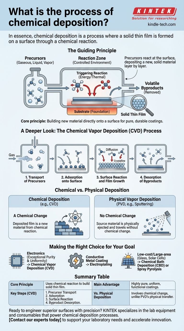
In essence, chemical deposition is a process where a solid thin film is formed on a surface, known as a substrate, through a chemical reaction. Gaseous, liquid, or vaporized chemical compounds, called precursors, are introduced into a controlled environment where they react at or near the substrate's surface, depositing a new, solid material layer by layer.
The core principle of chemical deposition is using a controlled chemical reaction to build a new material directly onto a surface. This allows for the creation of highly pure, durable, and functional coatings with precisely engineered properties.
The Guiding Principle: From Precursor to Solid Film
Chemical deposition fundamentally transforms starting chemicals into a solid film. This process is governed by three key elements.
The Starting Chemicals (Precursors)
Precursors are volatile compounds containing the elements you want to deposit. They are engineered to be stable until they reach the reaction zone.
These chemicals are typically delivered as a gas or a vaporized liquid into a reaction chamber.
The Foundation (The Substrate)
The substrate is the workpiece or material that receives the coating. Its surface provides the location for the chemical reactions to occur.
Often, the substrate is heated to provide the necessary energy to initiate and sustain the reactions.
Triggering the Chemical Reaction
The transformation from gas to solid film is triggered by energy. This energy, usually thermal, causes the precursor molecules to decompose or react with other gases.
This reaction forms nonvolatile (solid) products that deposit onto the substrate, while volatile byproducts are removed.
A Deeper Look: The Chemical Vapor Deposition (CVD) Process
Chemical Vapor Deposition (CVD) is the most common and illustrative example of this process. It can be broken down into several distinct steps.
Step 1: Transport of Precursors
Gaseous precursor chemicals are precisely introduced and transported into a reaction chamber, which often operates under a vacuum.
Step 2: Adsorption onto the Surface
The gas molecules land and stick to the hot substrate surface in a process called adsorption.
Step 3: Surface Reaction and Film Growth
The heat of the substrate provides the energy for the adsorbed precursor molecules to react. This surface-catalyzed reaction forms the solid film.
Molecules may diffuse across the surface to find optimal growth sites, leading to the nucleation and growth of a uniform, crystalline, or amorphous layer.
Step 4: Desorption of Byproducts
The chemical reaction also creates gaseous byproducts, which are no longer needed.
These byproducts detach from the surface (desorption) and are pumped away, leaving only the pure, desired film behind.
Understanding the Key Distinction: Chemical vs. Physical Deposition
It's critical to distinguish chemical deposition from its physical counterpart, as the underlying mechanisms are fundamentally different.
The Defining Factor: A Chemical Change
In all forms of chemical deposition, the deposited film is a new material created by a chemical reaction at the substrate. The precursors are consumed and transformed.
The Alternative: Physical Vapor Deposition (PVD)
Processes like sputtering are a form of Physical Vapor Deposition (PVD). In PVD, the source material is physically ejected (e.g., by ion bombardment) and travels to the substrate without a chemical change.
Think of PVD as spray-painting with atoms, whereas CVD is like building a structure brick by chemical brick.
Making the Right Choice for Your Goal
Different chemical deposition methods are suited for different applications, from semiconductor manufacturing to creating decorative coatings.
- If your primary focus is exceptional purity and uniformity for electronics: Chemical Vapor Deposition (CVD) provides the atomic-level control required for complex microchips.
- If your primary focus is applying a conductive metal coating: Electroplating is a highly efficient and well-established industrial method that uses an electric current.
- If your primary focus is low-cost or large-area application from a solution: Techniques like Chemical Bath Deposition (CBD) or spray pyrolysis offer economical alternatives for goals like coating glass or creating solar cells.
Ultimately, mastering chemical deposition allows engineers and scientists to design materials from the atom up, building the functional surfaces that power modern technology.
Summary Table:
| Key Aspect | Description |
|---|---|
| Core Principle | Uses a chemical reaction to build a solid thin film on a substrate. |
| Key Steps (CVD) | 1. Precursor Transport 2. Adsorption 3. Surface Reaction 4. Byproduct Desorption. |
| Main Advantage | Creates highly pure, uniform, and functional coatings with precise properties. |
| Vs. Physical Deposition (PVD) | Involves a chemical change to create a new material, unlike PVD's physical transfer. |
Ready to engineer superior surfaces with precision? KINTEK specializes in the lab equipment and consumables that power chemical deposition processes, from research to production. Whether you are developing next-generation semiconductors, durable protective coatings, or advanced functional materials, our expertise and solutions can help you achieve unparalleled purity and control. Contact our experts today to discuss how we can support your specific laboratory needs and accelerate your innovation.
Visual Guide
Related Products
- Chemical Vapor Deposition CVD Equipment System Chamber Slide PECVD Tube Furnace with Liquid Gasifier PECVD Machine
- HFCVD Machine System Equipment for Drawing Die Nano-Diamond Coating
- 915MHz MPCVD Diamond Machine Microwave Plasma Chemical Vapor Deposition System Reactor
- RF PECVD System Radio Frequency Plasma-Enhanced Chemical Vapor Deposition RF PECVD
- Microwave Plasma Chemical Vapor Deposition MPCVD Machine System Reactor for Lab and Diamond Growth
People Also Ask
- How are carbon nanotubes grown? Master Scalable Production with Chemical Vapor Deposition
- Why is Chemical Vapor Deposition (CVD) equipment uniquely suited for constructing hierarchical superhydrophobic structures?
- What is the chemical vapor deposition growth process? Build Superior Thin Films from the Atom Up
- What are the core advantages of PE-CVD in OLED encapsulation? Protect Sensitive Layers with Low-Temp Film Deposition
- How expensive is chemical vapor deposition? Understanding the True Cost of High-Performance Coating