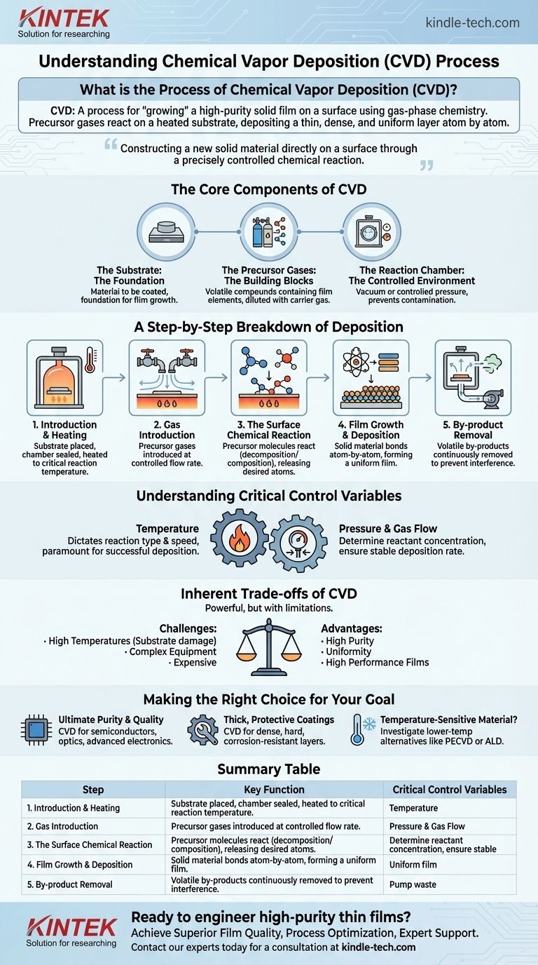
In essence, Chemical Vapor Deposition (CVD) is a process for "growing" a high-purity solid film on a surface using gas-phase chemistry. In a controlled chamber, volatile precursor gases are introduced and react on a heated object (the substrate), breaking down and depositing a thin, dense, and uniform layer of the desired material atom by atom.
The core principle of CVD is not simply applying a coating, but rather constructing a new solid material directly on a surface through a precisely controlled chemical reaction. This allows for the creation of exceptionally pure, high-performance films that are often impossible to produce by other means.
The Core Components of the CVD Process
To understand how CVD works, you must first understand its three essential components.
The Substrate: The Foundation
The substrate is the material or object that is to be coated. It is placed inside the reaction chamber and serves as the physical foundation upon which the new film will grow.
The Precursor Gases: The Building Blocks
Precursor gases are volatile chemical compounds that contain the specific elements required for the final film. These gases, often diluted with a non-reactive carrier gas, are the raw materials that will be chemically transformed into the solid coating.
The Reaction Chamber: The Controlled Environment
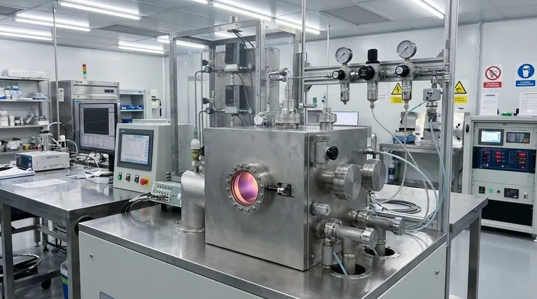
The entire process takes place within a reaction chamber, which is typically held under a vacuum or controlled pressure. This sealed environment prevents contamination and allows for precise control over the critical process variables.
A Step-by-Step Breakdown of Deposition
The CVD process follows a clear and repeatable sequence of events to build the desired film.
1. Introduction and Heating
First, the substrate is placed inside the chamber. The chamber is then sealed, and the substrate is heated to a specific, carefully controlled reaction temperature. This temperature is the most critical parameter in the entire process.
2. Gas Introduction
Once the substrate reaches the target temperature, the precursor gases are introduced into the chamber at a controlled flow rate. These gases flow over and around the heated substrate.
3. The Surface Chemical Reaction
When the hot precursor gas molecules come into contact with the heated substrate surface, they gain enough thermal energy to react. This reaction can be a decomposition (breaking down) or composition (combining) process that releases the desired solid atoms or molecules.
4. Film Growth and Deposition
The solid material released from the chemical reaction bonds directly to the substrate surface. This deposition occurs atom-by-atom or molecule-by-molecule, gradually building up a thin, dense, and highly uniform film across the entire exposed surface.
5. By-product Removal
The chemical reactions almost always create unwanted volatile by-products. These gaseous waste products are continuously removed from the chamber by the gas flow and a vacuum pump system, ensuring they do not interfere with the film growth.
Understanding the Critical Control Variables
The quality, thickness, and properties of the final film are not accidental; they are a direct result of meticulous control over the reaction environment.
The Role of Temperature
Substrate temperature is paramount. It dictates what kind of chemical reaction will occur and how fast it will proceed. A different temperature can result in a completely different material being deposited or no deposition at all.
The Impact of Pressure and Gas Flow
The pressure inside the chamber and the flow rate of the precursor gases determine the concentration of reactants available at the substrate surface. These variables are fine-tuned to ensure a stable and consistent deposition rate for a uniform coating.
Inherent Trade-offs of the CVD Process
While powerful, CVD is not without its limitations. The primary challenge is the requirement for high temperatures.
The elevated temperatures needed to trigger the chemical reaction can damage or alter the properties of certain substrates, particularly plastics or sensitive electronic components. Furthermore, the need for vacuum systems and precise control over gas flow and temperature makes CVD equipment relatively complex and expensive.
Making the Right Choice for Your Goal
Understanding the fundamentals of CVD allows you to determine if it is the right process for your specific application.
- If your primary focus is ultimate purity and crystalline quality: CVD is an exceptional choice for creating high-performance films for semiconductors, optics, and advanced electronics.
- If your primary focus is producing thick, protective coatings: The process excels at creating dense, hard, and corrosion-resistant layers on tools and industrial components.
- If your primary focus is coating a temperature-sensitive material: You should investigate lower-temperature alternatives like Plasma-Enhanced CVD (PECVD) or Atomic Layer Deposition (ALD), which use different energy sources to drive the reaction.
By mastering the interplay of chemistry, temperature, and pressure, you can leverage CVD to engineer materials with precisely controlled properties from the atomic level up.
Summary Table:
| CVD Process Step | Key Function | Critical Control Variables |
|---|---|---|
| 1. Introduction & Heating | Heat substrate to reaction temperature. | Substrate Temperature |
| 2. Gas Introduction | Introduce precursor gases into the chamber. | Gas Flow Rate, Pressure |
| 3. Surface Reaction | Precursor gases react on the hot substrate surface. | Temperature, Gas Concentration |
| 4. Film Growth | Solid material deposits atom-by-atom. | Deposition Rate, Uniformity |
| 5. By-product Removal | Remove gaseous waste from the chamber. | Vacuum/Flow System |
Ready to engineer high-purity, high-performance thin films for your lab?
The controlled, atom-by-atom deposition of Chemical Vapor Deposition is key to advancing research and development in semiconductors, optics, and protective coatings. KINTEK specializes in providing the precise lab equipment and consumables needed to master the CVD process.
We help you achieve:
- Superior Film Quality: Achieve the exceptional purity and uniformity critical for your most demanding applications.
- Process Optimization: Leverage equipment designed for meticulous control over temperature, pressure, and gas flow.
- Expert Support: Our team understands the complexities of deposition technologies and is here to support your lab's specific needs.
Let's discuss how our solutions can enhance your capabilities. Contact our experts today for a consultation.
Visual Guide
Related Products
- CVD Diamond Dressing Tools for Precision Applications
- Multi Heating Zones CVD Tube Furnace Machine Chemical Vapor Deposition Chamber System Equipment
- CVD Diamond Domes for Industrial and Scientific Applications
- CVD Diamond for Thermal Management Applications
- Chemical Vapor Deposition CVD Equipment System Chamber Slide PECVD Tube Furnace with Liquid Gasifier PECVD Machine
People Also Ask
- What is CVD diamond? The Ultimate Guide to Lab-Grown Diamonds and Their Uses
- How long does it take to make synthetic diamonds? Discover the 6-8 Week Science Behind Lab-Grown Gems
- How do CVD diamonds grow? A Step-by-Step Guide to Lab-Grown Diamond Creation
- What are the disadvantages of CVD diamonds? Understanding the trade-offs for your purchase.
- What color diamonds are CVD? Understanding the Process from Brown Tint to Colorless Beauty


