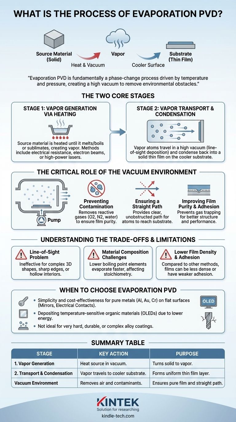
At its core, evaporation PVD is a process that uses heat to turn a solid material into a vapor within a high vacuum. This vapor then travels and condenses onto a cooler surface, known as the substrate, to form a precise, thin film. The entire method relies on changing the physical state of a source material—from solid to gas and back to solid—in a highly controlled environment.
Evaporation PVD is fundamentally a phase-change process driven by temperature and pressure. By creating a high vacuum, the process removes environmental obstacles, allowing vaporized atoms to travel in a straight line from a hot source to a cooler substrate, ensuring a pure and direct deposition.
The Two Core Stages of Evaporation
The entire process, while seemingly complex, can be understood as a sequence of two fundamental physical events. It is a direct journey from a source material to a finished film.
Stage 1: Vapor Generation via Heating
The process begins by heating a source material, often called the "target," inside a vacuum chamber. This material is heated until it reaches a temperature where it either melts and boils or sublimates directly from a solid into a gas.
This creates a cloud of vaporized atoms. The heating itself can be achieved through several methods, including electrical resistance heating (like a filament in a lightbulb), electron beams, or high-power lasers.
Stage 2: Vapor Transport and Condensation
Once in a gaseous state, the atoms travel away from the source. Because this occurs in a high vacuum, the atoms move in a straight path with few or no collisions, a principle known as line-of-sight deposition.
When these vaporized atoms strike the cooler substrate, they rapidly lose their thermal energy and condense back into a solid state. This progressive condensation builds up, layer by layer, to form a uniform thin film on any surface with a direct line of sight to the source.
The Critical Role of the Vacuum Environment
Performing evaporation in a high vacuum is not optional; it is essential for the success of the process. The vacuum addresses several critical challenges.
Preventing Contamination
A vacuum removes reactive gases like oxygen, nitrogen, and water vapor from the chamber. Without this step, these gases would react with the hot vapor, creating unwanted compounds and contaminating the final film.
Ensuring a Straight Path
In normal atmospheric pressure, the evaporated atoms would constantly collide with air molecules. This would scatter them randomly, preventing them from ever reaching the substrate in a controlled manner. A vacuum provides a clear, unobstructed path.
Improving Film Purity and Adhesion
By removing other gases, the vacuum ensures that only the source material is deposited onto the substrate. This prevents gases from becoming trapped within the growing film, which would compromise its structural integrity, density, and performance. Proper heating of the substrate can also be used to improve film adhesion and uniformity.
Understanding the Trade-offs and Limitations
While effective, evaporation PVD is not a universal solution. Its fundamental principles create specific limitations you must consider.
The "Line-of-Sight" Problem
Because the vapor travels in a straight line, evaporation can only coat surfaces that are directly visible from the source. It is highly ineffective for coating complex 3D shapes, sharp edges, or the interior of hollow objects.
Material Composition Challenges
When evaporating an alloy or compound with multiple elements, the element with the lower boiling point will evaporate more quickly. This can lead to a film whose chemical composition (stoichiometry) is different from that of the original source material.
Lower Film Density and Adhesion
Compared to other PVD methods like sputtering, the evaporated atoms arrive at the substrate with relatively low kinetic energy. This can sometimes result in films that are less dense or have weaker adhesion to the substrate, although this can be mitigated with substrate heating.
When to Choose Evaporation PVD
Your choice of a deposition technique should always be guided by the final goal of your project.
- If your primary focus is simplicity and cost-effectiveness for pure metals: Evaporation is often the most direct PVD method for depositing materials like aluminum, gold, or chromium onto flat substrates for applications like mirrors or electrical contacts.
- If your primary focus is depositing temperature-sensitive organic materials: The lower energy nature of thermal evaporation makes it ideal for materials, such as those used in OLED displays, that would be damaged by the high-energy ion bombardment found in other methods.
- If your primary focus is creating a very hard, durable, or complex alloy coating: You should look to other methods like sputtering, as evaporation struggles to maintain stoichiometry and produces films with lower density and adhesion.
Understanding these core principles allows you to select the right deposition technique based on your material, geometry, and desired film properties.
Summary Table:
| Stage | Key Action | Purpose |
|---|---|---|
| 1. Vapor Generation | Heat a source material in a vacuum. | Turns the solid material into a vapor. |
| 2. Transport & Condensation | Vapor travels and condenses on a cooler substrate. | Forms a uniform thin film layer by layer. |
| Vacuum Environment | Removes air and contaminants from the chamber. | Ensures a pure film and a straight-line deposition path. |
Ready to enhance your lab's capabilities with precise thin-film deposition?
At KINTEK, we specialize in providing high-quality lab equipment, including advanced PVD systems tailored to your research and production needs. Whether you are working with pure metals for electronics or temperature-sensitive materials for OLEDs, our solutions ensure purity, consistency, and reliability.
Let our experts help you select the ideal equipment to achieve superior film quality and improve your lab's efficiency.
Contact us today to discuss your specific application and discover the KINTEK advantage!
Visual Guide
Related Products
- Molybdenum Tungsten Tantalum Evaporation Boat for High Temperature Applications
- Inclined Rotary Plasma Enhanced Chemical Vapor Deposition PECVD Equipment Tube Furnace Machine
- Hemispherical Bottom Tungsten Molybdenum Evaporation Boat
- Vacuum Hot Press Furnace Machine for Lamination and Heating
- Aluminized Ceramic Evaporation Boat for Thin Film Deposition
People Also Ask
- What is the thermal evaporation technique? A Guide to Thin-Film Deposition for Your Lab
- What is thermal evaporation used to deposit? A Guide to Metals, Compounds, and Key Applications
- What is the widely used boat made of in thermal evaporation? Choosing the Right Material for High-Purity Deposition
- What is the difference between sputtering and thermal evaporation? Choose the Right PVD Method for Your Thin Film
- What is thermal effect via evaporation? A Simple Guide to Thin-Film Deposition