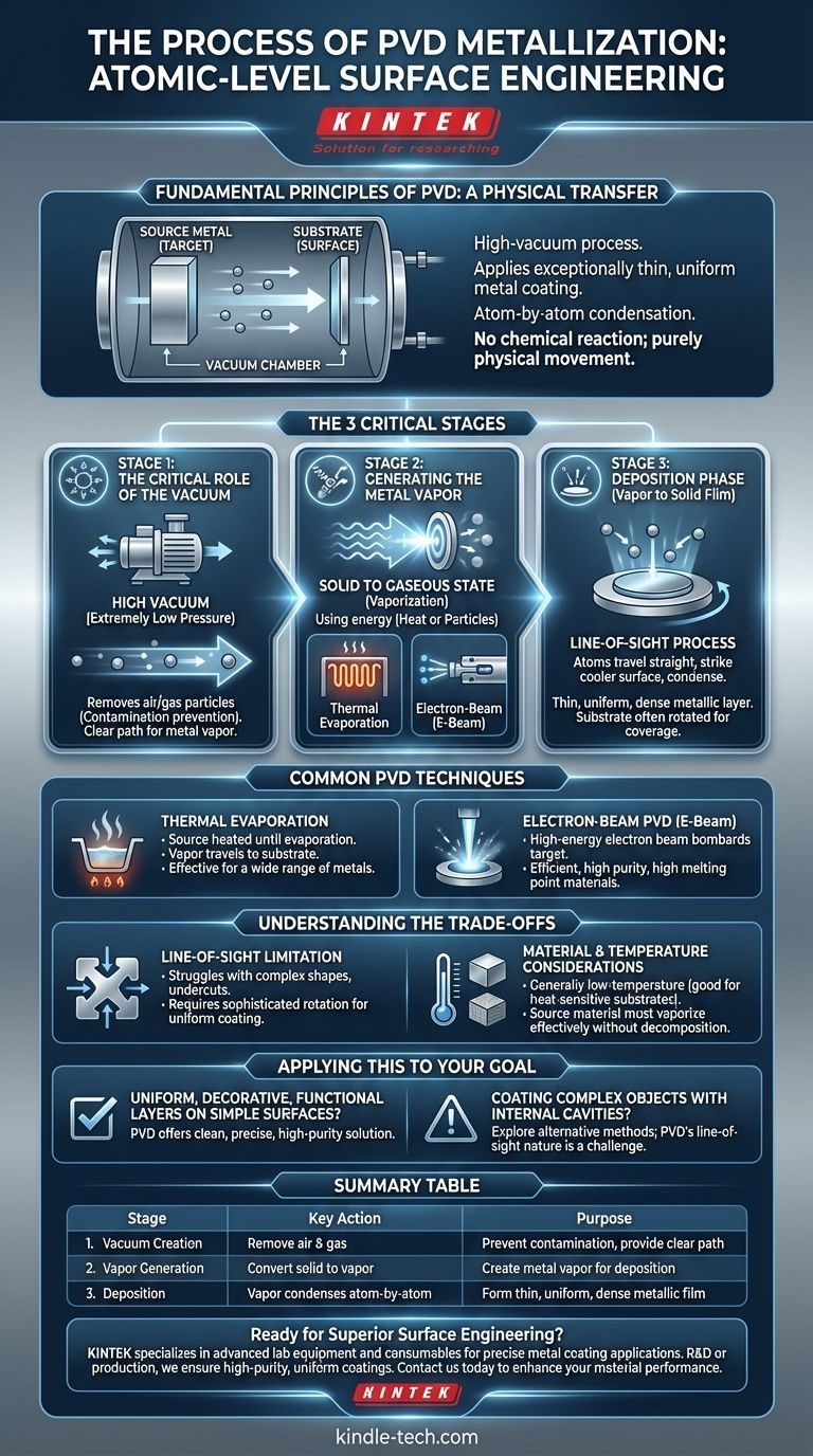
At its core, Physical Vapor Deposition (PVD) metallization is a high-vacuum process used to apply an exceptionally thin, uniform metal coating onto a surface, known as a substrate. The technique involves physically transforming a solid source metal into a vapor, which then travels through the vacuum and condenses atom by atom onto the substrate, forming the desired metallic film.
The crucial concept to grasp is that PVD is a purely physical transfer of material. Unlike chemical processes, no reaction occurs; the metal is simply moved from a source to a surface like spray-painting with individual atoms in a vacuum.
The Fundamental Principles of PVD
To understand PVD, it's best to break it down into its three essential stages. Each stage is critical for achieving a high-quality, pure metallic coating.
The Critical Role of the Vacuum
The entire PVD process takes place under a very high vacuum (extremely low pressure). This controlled environment is non-negotiable for two key reasons.
First, it removes air and other gas particles that would otherwise contaminate the metal film. Second, it gives the vaporized metal atoms a clear, unobstructed path from the source to the substrate.
Generating the Metal Vapor
Once the vacuum is established, the solid source material (the "target") must be converted into a gaseous state. This is the "vapor" in Physical Vapor Deposition.
This transformation is achieved using energy. Common methods include high-temperature evaporation or bombarding the target with high-energy particles like an electron beam.
The Deposition Phase: From Vapor to Solid Film
The vaporized metal atoms travel in a straight line from the source toward the substrate. This is often referred to as a line-of-sight process.
When these atoms strike the cooler surface of the substrate, they condense back into a solid state. This happens atom by atom, building up a very thin, uniform, and dense metallic layer. To ensure even coverage on complex shapes, the substrate is often rotated during this phase.
Common PVD Metallization Techniques
While the principle remains the same, the method used to generate the vapor can differ, leading to different techniques with specific advantages.
Thermal Evaporation
This is a common method where the source metal is heated in the vacuum chamber until it begins to evaporate. The resulting vapor then travels to and condenses on the substrate. It is effective for a wide range of metals.
Electron-Beam PVD (E-Beam)
In this more advanced technique, a high-energy beam of electrons is fired at the source material. This intense energy bombards the target, causing it to vaporize with high efficiency and purity. This method allows for the deposition of materials with very high melting points.
Understanding the Trade-offs
PVD is a powerful technique, but it's essential to recognize its operational characteristics and limitations.
The Line-of-Sight Limitation
Because the metal atoms travel in a straight line, PVD struggles to coat the inside of complex shapes or undercut areas. Achieving a uniform coating on a non-planar surface requires sophisticated substrate rotation and careful positioning.
Material and Temperature Considerations
The process is generally considered low-temperature compared to other coating methods, which is advantageous for heat-sensitive substrates. However, the choice of source material is critical, as it must be able to be vaporized effectively without decomposing.
Applying This to Your Goal
Choosing the right approach depends entirely on the requirements for the final coating.
- If your primary focus is a uniform, decorative, or functional metal layer on a relatively simple surface: PVD offers a clean, precise, and high-purity solution.
- If your primary focus is coating a highly complex object with internal cavities: You may need to explore alternative methods, as PVD's line-of-sight nature presents a significant challenge.
Ultimately, PVD metallization provides an exceptionally controlled method for engineering surfaces at the atomic level.
Summary Table:
| Stage | Key Action | Purpose |
|---|---|---|
| 1. Vacuum Creation | Remove air and gas particles | Prevent contamination and provide a clear path for vapor |
| 2. Vapor Generation | Convert solid metal to vapor via evaporation or e-beam | Create the metal vapor for deposition |
| 3. Deposition | Vapor condenses atom-by-atom onto substrate | Form a thin, uniform, and dense metallic film |
Ready to achieve superior surface engineering with PVD metallization? KINTEK specializes in advanced lab equipment and consumables for precise metal coating applications. Whether you're working on R&D or production, our solutions ensure high-purity, uniform coatings for your substrates. Contact us today to discuss how we can support your laboratory's PVD needs and enhance your material performance.
Visual Guide
Related Products
- Inclined Rotary Plasma Enhanced Chemical Vapor Deposition PECVD Equipment Tube Furnace Machine
- RF PECVD System Radio Frequency Plasma-Enhanced Chemical Vapor Deposition RF PECVD
- Vacuum Hot Press Furnace Machine for Lamination and Heating
- Chemical Vapor Deposition CVD Equipment System Chamber Slide PECVD Tube Furnace with Liquid Gasifier PECVD Machine
- VHP Sterilization Equipment Hydrogen Peroxide H2O2 Space Sterilizer
People Also Ask
- What is the difference between CVD and PECVD? Choose the Right Thin-Film Deposition Method
- What is plasma enhanced chemical vapour deposition process? Unlock Low-Temperature, High-Quality Thin Films
- What is plasma enhanced chemical vapor deposition? Achieve Low-Temperature, High-Quality Thin Films
- How does plasma enhanced CVD work? Achieve Low-Temperature, High-Quality Thin Film Deposition
- What is PECVD silicon deposition? Achieve Low-Temperature, High-Quality Thin Films