In essence, Physical Vapor Deposition (PVD) is a vacuum-based coating process that produces a thin, highly durable film on a substrate. The method involves physically transforming a solid source material into a vapor, which then travels through the vacuum chamber and condenses onto the target object, atom by atom. Because this process involves no chemical reactions, the resulting coating is a pure, high-performance layer.
The core principle of PVD is not to chemically alter a surface, but to physically "build" a new one on top of it. This precise, atom-by-atom deposition in a vacuum allows for the creation of extremely thin, functional, and durable coatings that are difficult to achieve through other methods.
How Does PVD Fundamentally Work?
The PVD process can be broken down into three critical stages that all occur under highly controlled vacuum conditions.
Step 1: Creating a Vacuum
The entire process takes place inside a vacuum chamber. Removing the air is crucial because it eliminates particles that could otherwise react with or impede the vaporized coating material.
Step 2: Generating the Vapor
A solid, pure source material—often called the "target"—is converted into a vapor. This is achieved through high-energy physical methods such as high-temperature evaporation or by bombarding the target with high-energy ions, a process known as sputtering.
Step 3: Transport and Deposition
The vaporized atoms travel in a straight line through the vacuum chamber and deposit onto the substrate (the object being coated). As the atoms land on the surface, they condense and build a thin, dense, and highly adherent film.
Why Choose PVD? The Key Advantages
Engineers and designers specify PVD coatings when the surface properties of a material are critical to its function or longevity.
Enhanced Durability and Hardness
PVD coatings are known for their ability to significantly increase the hardness of a surface. This enhancement reduces friction and improves resistance to wear and oxidation.
High-Temperature Performance
The process is ideal for creating coatings that must withstand extreme conditions. PVD films can improve a substrate's resistance to high temperatures and ablation, which is why they are common in aerospace technology.
Superior Adhesion and Finish
Because PVD physically bonds the coating to the substrate at an atomic level, the adhesion is excellent. The resulting film is also very thin and uniform, meaning it perfectly replicates the original surface texture, producing a brilliant metallic luster without any need for post-polishing.
Material Versatility
PVD can be used with a wide variety of materials, including metals, non-metals, and compounds. It is particularly effective for depositing materials that have very high melting points and would be difficult to work with using other methods.
Understanding the Trade-offs
While powerful, PVD is not a universal solution. Understanding its limitations is key to using it effectively.
Line-of-Sight Deposition
In most PVD processes, the coating material travels in a straight line from the source to the substrate. This means it is difficult to coat complex internal geometries or the undersides of objects without complex fixtures to rotate the parts during coating.
Equipment and Cost
PVD requires a significant capital investment in vacuum chambers and high-energy power sources. The complexity of the process means it is generally more expensive than simpler coating methods like painting or traditional electroplating.
Slower Deposition Rates
Compared to some conventional coating processes, PVD can be slower. While the resulting films are of very high quality, the time required can impact high-volume production throughput.
Where is PVD Used in Practice?
PVD's unique combination of durability and precision makes it valuable across a wide range of industries.
Functional and Technical Coatings
PVD is critical in the manufacturing of high-performance items. This includes semiconductor devices, thin-film solar panels, and diffusion barriers that prevent materials from migrating into one another.
Tooling and Industrial Applications
Cutting tools, drills, and molds are frequently coated with PVD to increase their hardness and reduce friction. This extends the tool's life and improves its performance.
Decorative and Consumer Finishes
The process is widely used to create durable and attractive finishes on consumer goods. Applications include jewelry, kitchen and bathroom hardware, marine supplies, and architectural glass coatings where both aesthetic appeal and resistance to wear are essential.
Making the Right Choice for Your Goal
Selecting a coating technology depends entirely on your project's primary objective.
- If your primary focus is performance and durability: PVD is an excellent choice for creating hard, low-friction, and temperature-resistant surfaces on critical components.
- If your primary focus is a premium aesthetic finish: PVD provides a durable, lustrous metallic coating for consumer products that is far superior to traditional painting or plating.
- If your primary focus is low cost for simple applications: You may find that conventional methods like painting or electroplating are more cost-effective, provided they meet your durability requirements.
Ultimately, PVD is a sophisticated tool for engineering surfaces with properties that are simply unattainable through more conventional means.
Summary Table:
| Aspect | PVD Coating Characteristic |
|---|---|
| Process Type | Physical (non-chemical), vacuum-based |
| Key Advantages | Extreme hardness, high-temperature resistance, superior adhesion |
| Common Applications | Cutting tools, semiconductors, decorative finishes |
| Primary Limitation | Line-of-sight deposition (complex geometries can be challenging) |
Ready to enhance your products with high-performance PVD coatings?
KINTEK specializes in providing advanced lab equipment and consumables for precise coating applications. Whether you're developing cutting-edge semiconductors or durable consumer goods, our solutions help you achieve superior surface properties.
Contact our experts today to discuss how we can support your laboratory's specific coating challenges and goals.
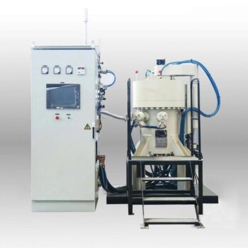
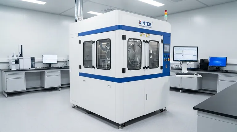
Visual Guide

Related Products
- RF PECVD System Radio Frequency Plasma-Enhanced Chemical Vapor Deposition RF PECVD
- Split Chamber CVD Tube Furnace with Vacuum Station Chemical Vapor Deposition System Equipment Machine
- Chemical Vapor Deposition CVD Equipment System Chamber Slide PECVD Tube Furnace with Liquid Gasifier PECVD Machine
- VHP Sterilization Equipment Hydrogen Peroxide H2O2 Space Sterilizer
- Molybdenum Tungsten Tantalum Special Shape Evaporation Boat
People Also Ask
- What are the benefits of PECVD? Achieve Superior Low-Temperature Thin Film Deposition
- What is an example of PECVD? RF-PECVD for High-Quality Thin Film Deposition
- Why is PECVD environment friendly? Understanding the Eco-Friendly Benefits of Plasma-Enhanced Coating
- Why does PECVD commonly use RF power input? For Precise Low-Temperature Thin Film Deposition
- What are the applications of PECVD? Essential for Semiconductors, MEMS, and Solar Cells