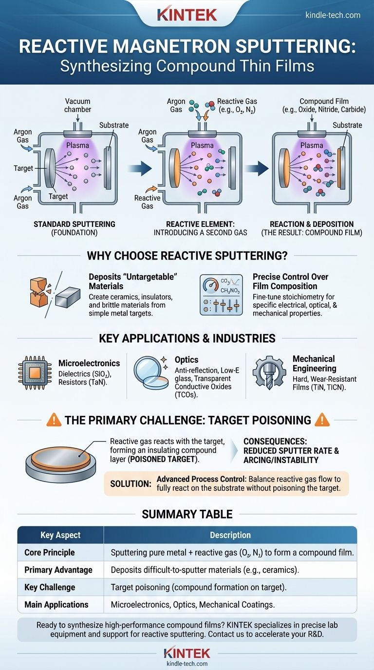
At its core, reactive magnetron sputtering is a thin-film deposition technique where a reactive gas, like oxygen or nitrogen, is intentionally introduced into the vacuum chamber during the sputtering process. This allows atoms from the primary material target to chemically react with the gas, forming a new compound material that deposits onto your substrate. It transforms the standard process of depositing a pure material into a method for creating complex compounds like oxides, nitrides, or carbides.
The essential takeaway is that reactive sputtering is not about depositing the material of the target itself. Instead, it uses the target material as a chemical ingredient, combining it with a reactive gas to synthesize a completely different compound material directly onto the surface of a substrate.
Deconstructing the Reactive Sputtering Process
To understand reactive sputtering, we must first briefly review the standard magnetron sputtering process it builds upon.
The Foundation: Standard Magnetron Sputtering
In a vacuum chamber, an inert gas like Argon is energized into a plasma. A powerful magnet confines this plasma near a source material, called the target.
Ions from the plasma are accelerated into the target, knocking off (or "sputtering") atoms. These sputtered atoms travel through the vacuum and condense on a substrate, gradually building up a thin film of the target material.
The "Reactive" Element: Introducing a Second Gas
This is the defining step. Alongside the inert Argon gas, a small, precisely controlled amount of a reactive gas (e.g., oxygen, nitrogen) is added to the chamber.
The process now contains both sputtered metal atoms from the target and reactive gas molecules.
The Result: Formation of a Compound Film
As the sputtered atoms travel toward the substrate, they react with the reactive gas. This chemical reaction can happen in the plasma, on the way to the substrate, or directly on the substrate surface itself.
The final film is therefore not the pure target material, but a compound. For example, sputtering a titanium target in a nitrogen environment produces a hard, gold-colored titanium nitride (TiN) film.
Why Choose Reactive Sputtering? The Core Advantage
The primary reason to use this method is its ability to create films from materials that are difficult, expensive, or impossible to manufacture as a solid sputter target.
Depositing Materials That Can't Be Targets
Many useful compounds, particularly ceramics like oxides and nitrides, are electrically insulating and brittle. This makes them poor candidates for a standard sputtering target, which should ideally be conductive and robust.
Reactive sputtering bypasses this problem by using an easy-to-fabricate, conductive pure metal target (e.g., silicon, titanium, aluminum) and simply adding the required gas (e.g., oxygen, nitrogen) to create the desired ceramic film (e.g., SiO₂, TiN, Al₂O₃).
Precise Control Over Film Composition
By carefully controlling the partial pressure of the reactive gas relative to the inert gas, you can fine-tune the stoichiometry of the resulting film. This allows for precise control over the material's electrical, optical, and mechanical properties.
Key Applications and Industries
This versatility makes reactive sputtering a cornerstone technology in several high-tech fields.
Microelectronics: Dielectrics and Resistors
The method is fundamental in semiconductor manufacturing for creating high-purity dielectric layers, such as silicon dioxide (SiO₂), and resistive films like tantalum nitride (TaN).
Optics: Functional and Protective Coatings
Reactive sputtering is used to deposit multi-layer anti-reflection coatings, low-emissivity films for energy-efficient glass, and transparent conductive oxides (TCOs) for displays and solar cells.
Mechanical Engineering: Hard and Wear-Resistant Films
The deposition of super-hard films like titanium nitride (TiN) and titanium carbonitride (TiCN) on cutting tools, drills, and mechanical components dramatically improves their lifespan and performance.
Understanding the Primary Challenge: Target Poisoning
The power of reactive sputtering comes with a significant process control challenge known as "target poisoning."
What Is Target Poisoning?
The reactive gas doesn't just react with sputtered atoms on the substrate; it also reacts with the surface of the sputtering target itself. This forms a thin, insulating compound layer (e.g., an oxide or nitride) on the metallic target.
The Consequences: Arcing and Instability
This "poisoned" layer has two negative effects. First, it dramatically reduces the sputter rate because it is harder to sputter atoms from a compound than from a pure metal. Second, if the layer is an electrical insulator, it can lead to charge buildup and destructive arcing, causing process instability and defects in the film.
The Solution: Advanced Process Control
Managing reactive sputtering requires a delicate balance. The goal is to supply just enough reactive gas to fully react with the atoms on the substrate, but not so much that it significantly poisons the target. This is often achieved with sophisticated feedback loops that monitor the process and dynamically adjust gas flow rates.
How to Apply This to Your Goal
Choosing the right sputtering method depends entirely on the film you intend to create.
- If your primary focus is depositing a pure metal or a metallic alloy: Use standard (non-reactive) magnetron sputtering with a target of the desired material.
- If your primary focus is depositing a compound like an oxide, nitride, or carbide: Reactive magnetron sputtering is almost always the most efficient and cost-effective choice.
- If your primary focus is high-volume industrial production of a compound film: Use reactive sputtering, but invest in a system with advanced process control to manage target poisoning and ensure run-to-run consistency.
Ultimately, reactive sputtering empowers you to synthesize complex materials that would otherwise be out of reach, making it one of the most versatile tools in surface engineering.
Summary Table:
| Key Aspect | Description |
|---|---|
| Core Principle | Sputtering a pure metal target in a reactive gas (e.g., O₂, N₂) to form a compound film (e.g., oxide, nitride). |
| Primary Advantage | Deposits materials that are difficult or impossible to use as solid sputter targets (e.g., insulating ceramics). |
| Key Challenge | Target poisoning, where a compound layer forms on the target, reducing sputter rate and causing instability. |
| Main Applications | Microelectronics (dielectrics), optics (anti-reflective coatings), mechanical engineering (hard, wear-resistant films). |
Ready to synthesize high-performance compound films in your lab?
KINTEK specializes in providing the precise lab equipment and expert support needed for advanced deposition processes like reactive magnetron sputtering. Whether you are developing new semiconductor components, optical coatings, or wear-resistant surfaces, our solutions help you achieve superior film quality and process control.
Contact KINTEK today to discuss your project and discover how our expertise in lab equipment and consumables can accelerate your research and development.
Visual Guide
Related Products
- RF PECVD System Radio Frequency Plasma-Enhanced Chemical Vapor Deposition RF PECVD
- Spark Plasma Sintering Furnace SPS Furnace
- Chemical Vapor Deposition CVD Equipment System Chamber Slide PECVD Tube Furnace with Liquid Gasifier PECVD Machine
- Microwave Plasma Chemical Vapor Deposition MPCVD Machine System Reactor for Lab and Diamond Growth
- Cylindrical Resonator MPCVD Machine System Reactor for Microwave Plasma Chemical Vapor Deposition and Lab Diamond Growth
People Also Ask
- What is plasma chemical vapor deposition? A Low-Temperature Thin Film Coating Solution
- What is plasma enhanced chemical vapour deposition process? Unlock Low-Temperature, High-Quality Thin Films
- How does Radio Frequency Enhanced Plasma Chemical Vapour Deposition (RF-PECVD) work? Learn the Core Principles
- What is the role of RF-PECVD in VFG preparation? Mastering Vertical Growth and Surface Functionality
- What is plasma enhanced chemical Vapour deposition process used for fabrication of? A Guide to Low-Temperature Thin Films


