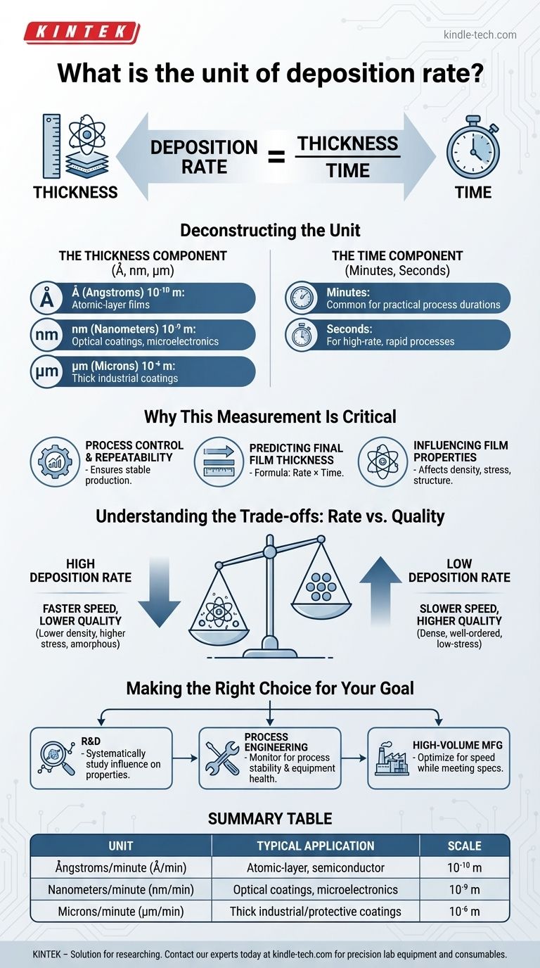
The standard unit for deposition rate is a measure of thickness per unit of time. It is most commonly expressed in Angstroms per minute (Å/min) or nanometers per minute (nm/min), particularly in fields like semiconductor manufacturing and materials science research where atomic-level precision is required.
Deposition rate is more than just a measurement; it is a critical process parameter that quantifies the speed of film growth. Understanding its units is the first step toward controlling the thickness, quality, and final properties of any deposited material.
Deconstructing the Unit: Thickness Over Time
At its core, the unit for deposition rate is fundamentally simple: a unit of length (or thickness) divided by a unit of time. The specific units chosen depend on the context of the process and the required precision.
The Thickness Component (Å, nm, µm)
The choice of the thickness unit reflects the scale of the film being created.
- Angstroms (Å): One Angstrom is 0.1 nanometers, or 10⁻¹⁰ meters. This unit is used when discussing films that are only a few atomic layers thick, common in advanced research and semiconductor fabrication.
- Nanometers (nm): A nanometer is 10⁻⁹ meters. It is the most common unit in thin-film applications like optical coatings and microelectronics.
- Microns (µm): A micron (or micrometer) is 10⁻⁶ meters. This larger unit is typically reserved for thicker industrial coatings, such as protective layers or metallization for packaging.
The Time Component (Minutes or Seconds)
The time component is usually chosen for practical convenience during the deposition run.
- Minutes: This is the most common unit because many deposition processes take several minutes to hours to complete. A rate per minute provides a practical and easily understood number.
- Seconds: For very high-rate processes or very short depositions, a rate measured in nanometers per second (nm/s) may be more appropriate to capture rapid changes.
Why This Measurement Is Critical
Understanding the deposition rate is essential for achieving reliable and repeatable results. It is one of the most important variables in any thin-film deposition process.
Process Control and Repeatability
By monitoring the deposition rate in real-time with instruments like a quartz crystal microbalance (QCM), engineers can ensure a process is stable and repeatable from one run to the next.
Predicting Final Film Thickness
The relationship is straightforward: Final Thickness = Deposition Rate × Time. This simple formula allows operators to precisely control the final thickness of a film by managing the duration of the deposition.
Influencing Film Properties
The speed at which atoms arrive at a surface directly impacts how they arrange themselves. Therefore, the deposition rate is a powerful lever for influencing a film's final material properties, such as density, internal stress, and crystalline structure.
Understanding the Trade-offs: Rate vs. Quality
Choosing a deposition rate is not simply about going as fast as possible. It involves a critical trade-off between manufacturing speed and the quality of the resulting film.
The Impact of High Deposition Rates
A high deposition rate increases manufacturing throughput, which is crucial for commercial production. However, it can lead to films with lower density, higher internal stress, and a more disordered (amorphous) structure because atoms have less time to settle into ideal energetic positions.
The Benefits of Low Deposition Rates
Slower deposition rates generally produce higher-quality films. The arriving atoms have more time and surface mobility to form dense, well-ordered, and low-stress layers. This is often required for high-performance applications like precision optics or advanced electronics.
Making the Right Choice for Your Goal
The "correct" deposition rate is entirely dependent on your application. Your goal determines how you should interpret and use this critical parameter.
- If your primary focus is research and development: Treat deposition rate as a key independent variable to systematically study its influence on film properties like crystallinity, stress, and stoichiometry.
- If your primary focus is process engineering: Monitor deposition rate as the most important real-time indicator of process stability and equipment health.
- If your primary focus is high-volume manufacturing: Optimize for the highest possible deposition rate that still reliably meets the minimum specifications for film quality, uniformity, and performance.
Ultimately, mastering the deposition rate is about translating a simple measurement of speed into precise control over your final material's structure and function.
Summary Table:
| Unit | Typical Application | Scale |
|---|---|---|
| Ångstroms/minute (Å/min) | Atomic-layer films, semiconductor fabrication | 10⁻¹⁰ meters |
| Nanometers/minute (nm/min) | Optical coatings, microelectronics (most common) | 10⁻⁹ meters |
| Microns/minute (µm/min) | Thick industrial/protective coatings | 10⁻⁶ meters |
Need precise control over your deposition process? The right deposition rate is key to achieving the film thickness, quality, and uniformity your application demands. At KINTEK, we specialize in providing the lab equipment and consumables—from quartz crystal monitors to deposition systems—that help researchers and engineers master this critical parameter. Whether you're in R&D or high-volume manufacturing, our solutions are designed to ensure process stability and repeatability. Contact our experts today to discuss how we can support your specific laboratory needs and help you optimize your thin-film deposition results.
Visual Guide