In essence, RF sputtering is used to deposit thin films of electrically insulating materials. While other methods like DC sputtering work well for conductive metals, they fail when the target material is an insulator. RF sputtering overcomes this fundamental limitation, making it an essential process for creating advanced thin films for semiconductors, optical devices, and other high-tech applications.
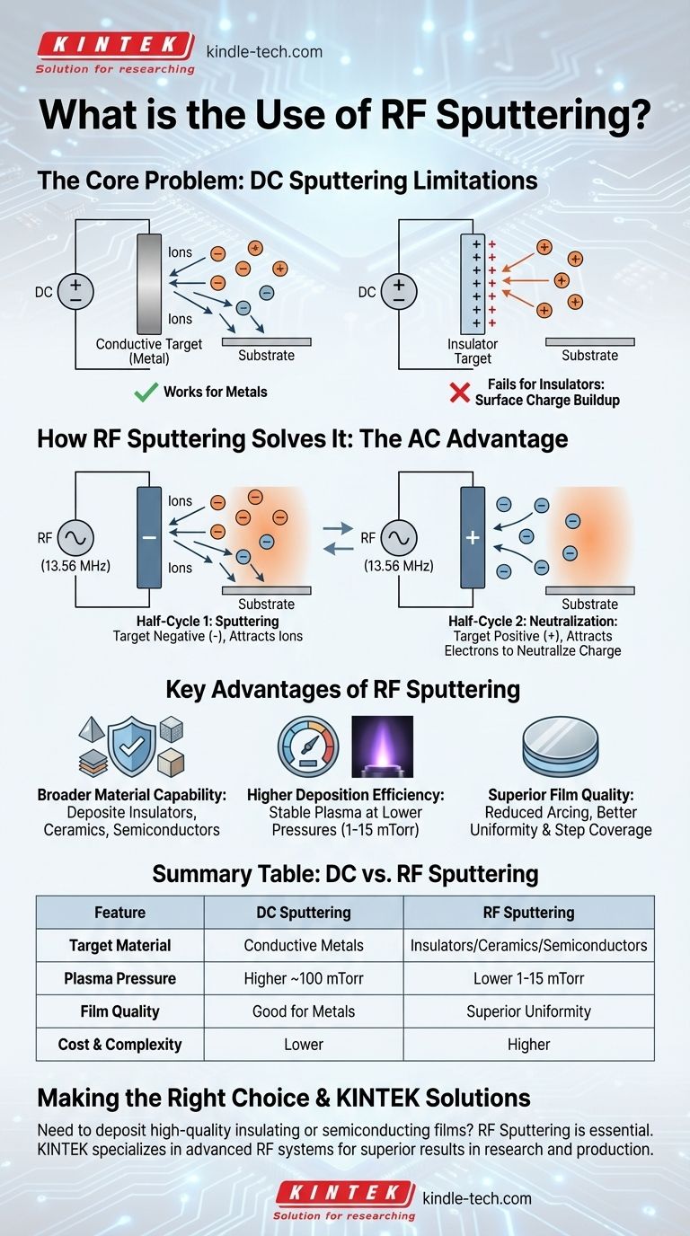
The core problem with sputtering non-conductive materials is that the target's surface accumulates a positive charge, repelling the very ions needed for the process to continue. RF sputtering solves this by using an alternating (AC) power source, which periodically neutralizes this charge buildup and allows for a stable, continuous deposition.
The Core Problem: Sputtering Insulators
Sputtering is a physical vapor deposition (PVD) technique where atoms are ejected from a solid target material by bombarding it with energetic ions in a vacuum. These ejected atoms then travel and deposit onto a substrate, forming a thin film.
The Limitation of DC Sputtering
For electrically conductive targets, the simplest method is Direct Current (DC) sputtering. A high negative DC voltage is applied to the target, attracting positive ions (like Argon) from the plasma.
These ions strike the target with enough force to knock atoms loose. However, if the target is an insulator (a dielectric material), this process quickly breaks down.
Why DC Fails with Non-conductors
When positive ions bombard a non-conductive target, they cannot be neutralized by a flow of electrons from the power supply. Instead, a layer of positive charge builds up on the target's surface.
This "surface charging" effect effectively creates a shield that repels incoming positive ions, halting the sputtering process almost immediately.
How RF Sputtering Solves the Problem
RF sputtering replaces the DC power supply with a high-frequency Radio Frequency (RF) AC power source, typically operating at 13.56 MHz. This alternating voltage is the key to sputtering insulators.
The Two-Cycle Mechanism
The RF field creates an oscillating plasma. In one half of the AC cycle, the target becomes negatively charged, attracting positive ions and causing sputtering just like in the DC process.
In the other half-cycle, the target becomes positively charged. During this brief period, it attracts a flood of highly mobile electrons from the plasma, which neutralizes the positive charge built up from the previous half-cycle. This prevents the "shielding" effect and allows sputtering to continue indefinitely.
Key Advantages of RF Sputtering
This alternating mechanism provides several significant advantages over other deposition techniques, especially when working with challenging materials.
Broader Material Capability
The primary benefit is the ability to deposit materials that are impossible to sputter with DC systems. This includes a vast range of insulators, ceramics, and semiconductors used in modern electronics and optics.
Higher Deposition Efficiency
The oscillating electrons in the RF plasma are more energetic and cause more ionization within the chamber gas. This allows a stable plasma to be sustained at much lower pressures (1-15 mTorr).
Operating at lower pressure means sputtered atoms encounter fewer gas collisions on their way to the substrate, leading to a more efficient deposition and better film quality.
Superior Film Quality
RF sputtering produces films with excellent characteristics. The process reduces arcing and charge buildup, resulting in more uniform films with better step coverage over complex substrate topographies. It also minimizes issues like "race track erosion" on the target, leading to more stable, long-term process control.
Understanding the Trade-offs
While powerful, RF sputtering is not always the default choice. The primary trade-off is system complexity and cost.
RF power supplies and their associated impedance-matching networks are significantly more complex and expensive than their DC counterparts. This added complexity requires more sophisticated process control and maintenance.
For simple metal deposition where high throughput is the main goal, DC sputtering is often the more cost-effective solution. RF is chosen when material properties or film quality requirements demand it.
Making the Right Choice for Your Goal
Selecting the correct sputtering technique depends entirely on your material and desired outcome.
- If your primary focus is depositing conductive metals cost-effectively: DC sputtering is usually the more practical and economical choice.
- If your primary focus is depositing insulating or semiconducting materials: RF sputtering is the necessary and superior technology.
- If your primary focus is achieving the highest film quality and uniformity, especially at low pressures: RF sputtering offers better process control and deposition efficiency.
Ultimately, RF sputtering is the essential tool that enables the fabrication of complex devices from a wide palette of non-conductive materials.
Summary Table:
| Feature | DC Sputtering | RF Sputtering |
|---|---|---|
| Target Material | Conductive Metals | Insulators, Ceramics, Semiconductors |
| Plasma Pressure | Higher (~100 mTorr) | Lower (1-15 mTorr) |
| Film Quality | Good for metals | Superior uniformity & step coverage |
| Cost & Complexity | Lower | Higher |
Need to deposit high-quality insulating or semiconducting thin films? KINTEK specializes in advanced lab equipment, including RF sputtering systems, to help you achieve superior film quality and process control for your research and production. Let our experts help you select the right tool for your material science challenges. Contact our team today to discuss your specific needs!
Visual Guide
Related Products
- RF PECVD System Radio Frequency Plasma-Enhanced Chemical Vapor Deposition RF PECVD
- Horizontal High Temperature Graphite Vacuum Graphitization Furnace
- Spark Plasma Sintering Furnace SPS Furnace
- Automatic Laboratory Hydraulic Press for XRF & KBR Pellet Press
- Electron Beam Evaporation Coating Oxygen-Free Copper Crucible and Evaporation Boat
People Also Ask
- What is the role of RF-PECVD in VFG preparation? Mastering Vertical Growth and Surface Functionality
- How does plasma enhance CVD? Unlock Low-Temperature, High-Quality Film Deposition
- Why is a Matching Network Indispensable in RF-PECVD for Siloxane Films? Ensure Stable Plasma and Uniform Deposition
- What is plasma enhanced chemical Vapour deposition process used for fabrication of? A Guide to Low-Temperature Thin Films
- How does Radio Frequency Enhanced Plasma Chemical Vapour Deposition (RF-PECVD) work? Learn the Core Principles


