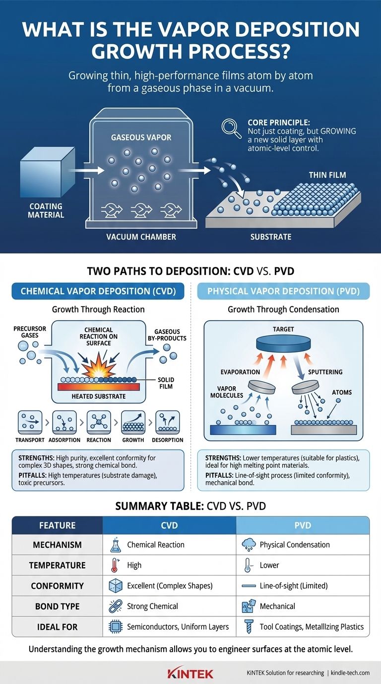
In short, vapor deposition is a family of processes used to apply a very thin, high-performance film of solid material onto a surface, known as a substrate. This is achieved by converting the coating material into a gaseous vapor inside a vacuum chamber, which then travels and condenses or reacts on the substrate's surface, building the film atom by atom. The two primary methods for this are Chemical Vapor Deposition (CVD) and Physical Vapor Deposition (PVD).
The core principle of vapor deposition is not simply coating a surface, but rather growing a new solid layer on it from a gaseous phase. This allows for unparalleled control over the material's purity, thickness, and structural properties at a microscopic level.
The Fundamental Principle: Building from the Vapor Phase
The goal of vapor deposition is to create ultra-thin films with specific, enhanced properties, such as hardness, corrosion resistance, or electrical conductivity. The process always takes place within a controlled vacuum chamber.
This vacuum environment is critical. It removes unwanted particles that could contaminate the film and allows the vaporized coating molecules to travel freely from their source to the substrate without obstruction.
The "growth" happens when these vapor molecules arrive at the substrate and transition back into a solid state, forming a dense, strongly bonded layer. How this transition occurs is the key difference between the two main types of vapor deposition.
Two Paths to Deposition: CVD vs. PVD
While both processes build a film from a vapor, they use fundamentally different mechanisms to generate that vapor and bond it to the surface.
Chemical Vapor Deposition (CVD): Growth Through Reaction
In CVD, the film is a product of a chemical reaction that occurs directly on the substrate's surface.
The process begins by introducing one or more volatile gas molecules, known as precursors, into the chamber. These precursors contain the atoms needed for the final film.
The substrate is heated to a precise reaction temperature. When the precursor gases come into contact with the hot surface, they decompose or react with each other.
This reaction forms the desired solid material, which deposits onto the substrate, while any unwanted chemical by-products remain in a gaseous state and are pumped out of the chamber.
The CVD process follows several distinct stages:
- Transport: Precursor gases are carried to the substrate.
- Adsorption: Gas molecules physically stick to the substrate's surface.
- Reaction: The heat energizes the molecules, causing them to chemically react and form a new solid.
- Growth: The solid nucleates and grows, building up the film layer by layer.
- Desorption: Gaseous by-products detach from the surface and are removed.
Physical Vapor Deposition (PVD): Growth Through Condensation
In PVD, the coating material starts as a solid target inside the vacuum chamber. It is converted into a vapor through purely physical means, travels to the substrate, and condenses back into a solid film. No chemical reaction is intended.
Two common PVD methods are:
- Evaporation: The solid source material is heated until it evaporates into a gas. This vapor then travels through the vacuum and condenses onto the cooler substrate, much like water vapor forming dew on a cold surface.
- Sputtering: The source material (or "target") is bombarded with high-energy ions. This bombardment acts like a microscopic sandblaster, physically knocking atoms off the target. These ejected atoms then travel and deposit onto the substrate.
Understanding the Trade-offs
Choosing between CVD and PVD depends entirely on the desired film properties, the substrate material, and the specific application.
Strengths of CVD
CVD excels at creating highly pure, dense, and uniform films. Because the precursor is a gas, it can flow into and coat complex, non-line-of-sight surfaces and intricate geometries with exceptional conformity. The chemical bond formed with the substrate is typically very strong.
Common Pitfalls of CVD
The high temperatures often required for the chemical reaction can damage heat-sensitive substrates. The precursor chemicals can also be highly toxic or corrosive, requiring careful handling and disposal of by-products.
Strengths of PVD
PVD is a lower-temperature process, making it suitable for a wider range of substrates, including plastics and other heat-sensitive materials. It is excellent for depositing materials with very high melting points that are difficult to vaporize chemically.
Common Pitfalls of PVD
PVD is generally a "line-of-sight" process, meaning it can be difficult to uniformly coat complex shapes or the insides of hollow parts. While adhesion is good, the bond is typically mechanical rather than chemical, which may be a limitation for some applications.
Making the Right Choice for Your Goal
Your decision should be guided by the end result you need to achieve.
- If your primary focus is creating a high-purity, crystalline semiconductor film: CVD is the industry standard due to its precise control over chemical purity and crystal structure.
- If your primary focus is applying a hard, wear-resistant coating onto a metal tool: PVD, particularly sputtering, is often preferred for its ability to deposit durable ceramic and metallic films at lower temperatures.
- If your primary focus is coating a complex 3D part with a uniform protective layer: CVD is the superior choice because the precursor gas can penetrate and coat all exposed surfaces evenly.
- If your primary focus is metallizing a plastic part for decorative or shielding purposes: PVD is the go-to method, as the low process temperature will not melt or warp the substrate.
By understanding the fundamental mechanism of growth, you can select the process that engineers your material's surface at the atomic level to meet your precise performance goals.
Summary Table:
| Feature | Chemical Vapor Deposition (CVD) | Physical Vapor Deposition (PVD) |
|---|---|---|
| Mechanism | Chemical reaction on the substrate surface | Physical condensation of vaporized material |
| Temperature | High (can damage sensitive substrates) | Lower (suitable for plastics, etc.) |
| Coating Conformity | Excellent for complex, 3D shapes | Line-of-sight; limited for complex geometries |
| Bond Type | Strong chemical bond | Mechanical bond |
| Ideal For | High-purity semiconductors, uniform protective layers | Hard coatings on tools, metallizing plastics |
Ready to engineer your material's surface at the atomic level?
KINTEK specializes in providing advanced lab equipment and consumables for vapor deposition processes. Whether you are developing semiconductors, applying wear-resistant coatings, or metallizing components, our solutions deliver the precision, purity, and performance your laboratory demands.
Contact our experts today to discuss how we can support your specific CVD or PVD application and help you achieve your precise performance goals.
Visual Guide
Related Products
- Chemical Vapor Deposition CVD Equipment System Chamber Slide PECVD Tube Furnace with Liquid Gasifier PECVD Machine
- HFCVD Machine System Equipment for Drawing Die Nano-Diamond Coating
- Customer Made Versatile CVD Tube Furnace Chemical Vapor Deposition Chamber System Equipment
- Inclined Rotary Plasma Enhanced Chemical Vapor Deposition PECVD Equipment Tube Furnace Machine
- Inclined Rotary Plasma Enhanced Chemical Vapor Deposition PECVD Equipment Tube Furnace Machine
People Also Ask
- What are the core advantages of PE-CVD in OLED encapsulation? Protect Sensitive Layers with Low-Temp Film Deposition
- What happens during deposition chemistry? Building Thin Films from Gaseous Precursors
- What are the processes of vapor phase deposition? Understand CVD vs. PVD for Superior Thin Films
- What is the chemical vapor deposition growth process? Build Superior Thin Films from the Atom Up
- What are the advantages of chemical vapor deposition? Achieve Superior Thin Films for Your Lab


