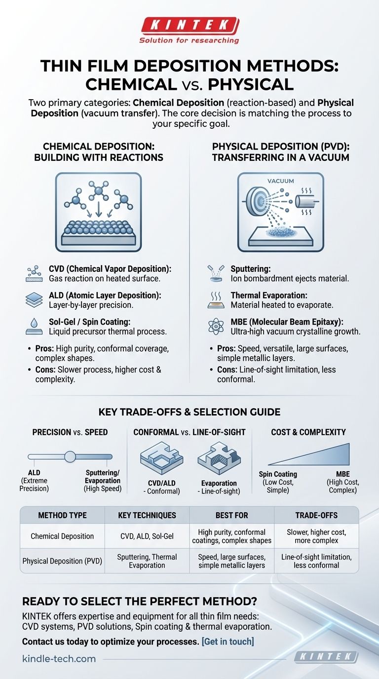
In short, thin films are made using a variety of deposition methods that fall into two primary categories: Chemical Deposition and Physical Deposition. These processes involve either inducing a chemical reaction on a surface to grow a film or physically transferring material onto a surface within a vacuum.
The core decision is not about finding a single "best" method, but about matching the process to the goal. Chemical methods build films through surface reactions, offering incredible precision, while physical methods transfer solid material, often providing speed and versatility.
The Two Fundamental Approaches to Deposition
To understand how thin films are made, it's essential to grasp the fundamental difference between the two main families of techniques. The choice of method dictates the film's purity, structure, thickness, and ultimately, its function.
Chemical Deposition: Building Films with Reactions
Chemical deposition methods use a chemical reaction at the substrate's surface to form the film. Precursor materials, typically in gas or liquid form, are introduced to a chamber where they react and deposit a solid layer onto the target object.
These methods are renowned for creating highly pure and uniform films that conform perfectly to the underlying surface, even on complex shapes.
The most common chemical methods include:
- Chemical Vapor Deposition (CVD): Precursor gases react on a heated substrate to form the film.
- Atomic Layer Deposition (ALD): A variation of CVD that deposits material one atomic layer at a time, offering unparalleled precision.
- Sol-Gel / Spin Coating: Liquid precursors are applied to a surface (often by spinning), and a subsequent thermal process creates the solid film.
Physical Deposition: Transferring Material in a Vacuum
Physical Deposition, often called Physical Vapor Deposition (PVD), involves physically moving material from a source target onto the substrate. This process happens in a vacuum to ensure purity.
The source material is converted into a vapor through methods like heating or ion bombardment. This vapor then travels through the vacuum chamber and condenses on the substrate, forming the thin film.
Common physical methods include:
- Sputtering: A target is bombarded with high-energy ions, which ejects or "sputters" atoms that then coat the substrate.
- Thermal Evaporation: A source material is heated in a vacuum until it evaporates, with the vapor condensing onto the cooler substrate.
Understanding the Trade-offs
No single deposition method is perfect for every situation. The optimal choice always involves balancing precision, speed, cost, and the specific materials being used.
Precision vs. Speed
Atomic Layer Deposition (ALD) offers the ultimate control, allowing for films to be built with single-atom-layer precision. This, however, is a very slow process.
In contrast, methods like sputtering or thermal evaporation can deposit material much more quickly, making them ideal for manufacturing processes where throughput is a key concern.
Conformal Coverage vs. Line-of-Sight
Chemical methods like CVD and ALD excel at creating conformal coatings, meaning the film's thickness is perfectly uniform, even over complex, three-dimensional surfaces.
Physical methods like evaporation are "line-of-sight" processes. The vapor travels in a straight line from the source to the substrate, making it difficult to evenly coat complex shapes or the sides of features.
Cost and Complexity
Simpler, solution-based methods like spin coating are relatively inexpensive and straightforward, making them common in research labs.
On the other end of the spectrum, advanced techniques like Molecular Beam Epitaxy (MBE) require ultra-high vacuum and sophisticated equipment, making them extremely expensive and complex to operate.
Selecting the Right Method for Your Application
Your choice of deposition method should be driven entirely by the intended use of the thin film.
- If your primary focus is cutting-edge semiconductor devices: You need the extreme precision of Atomic Layer Deposition (ALD) or the high-purity crystalline films from Molecular Beam Epitaxy (MBE).
- If your primary focus is coating large surfaces cost-effectively (e.g., anti-reflective glass or decorative finishes): The speed and versatility of magnetron sputtering is the industry standard.
- If your primary focus is creating optical coatings or simple metallic layers for electronics: Thermal evaporation offers a reliable and well-understood balance of cost and quality.
- If your primary focus is research and development with polymer or organic materials (e.g., OLEDs or flexible solar cells): The simplicity and low cost of spin coating or dip coating is often the best starting point.
Ultimately, understanding the core principles of chemical and physical deposition empowers you to choose the right tool for the job.
Summary Table:
| Method Type | Key Techniques | Best For | Trade-offs |
|---|---|---|---|
| Chemical Deposition | CVD, ALD, Sol-Gel | High purity, conformal coatings, complex shapes | Slower, higher cost, more complex |
| Physical Deposition (PVD) | Sputtering, Thermal Evaporation | Speed, large surfaces, simple metallic layers | Line-of-sight limitation, less conformal |
Ready to Select the Perfect Thin Film Deposition Method for Your Lab?
Choosing the right deposition technique is critical for your project's success. Whether you need the atomic-level precision of ALD for semiconductor research or the high-throughput capabilities of sputtering for industrial coatings, KINTEK has the expertise and equipment to support your goals.
We specialize in providing lab equipment and consumables for all your thin film needs, including:
- Chemical Vapor Deposition (CVD) systems
- Physical Vapor Deposition (PVD) solutions
- Spin coating and thermal evaporation equipment
Contact us today to discuss your specific application and let our experts help you optimize your thin film processes. Get in touch via our contact form for a personalized consultation!
Visual Guide
Related Products
- Aluminized Ceramic Evaporation Boat for Thin Film Deposition
- Tungsten Evaporation Boat for Thin Film Deposition
- Electron Beam Evaporation Coating Oxygen-Free Copper Crucible and Evaporation Boat
- Molybdenum Tungsten Tantalum Evaporation Boat for High Temperature Applications
- Vacuum Hot Press Furnace Machine for Lamination and Heating
People Also Ask
- What are thin films deposited by evaporation? A Guide to High-Purity Coating
- Why are high-purity ceramic boats used for lignin activation? Ensure Purity & Thermal Stability
- What is thin film deposition? Unlock Advanced Surface Engineering for Your Materials
- What is the chemical method for thin film deposition? Build Films from the Molecular Level Up
- Why is an alumina boat selected for catalyst precursors? Ensure Sample Purity at 1000 °C


