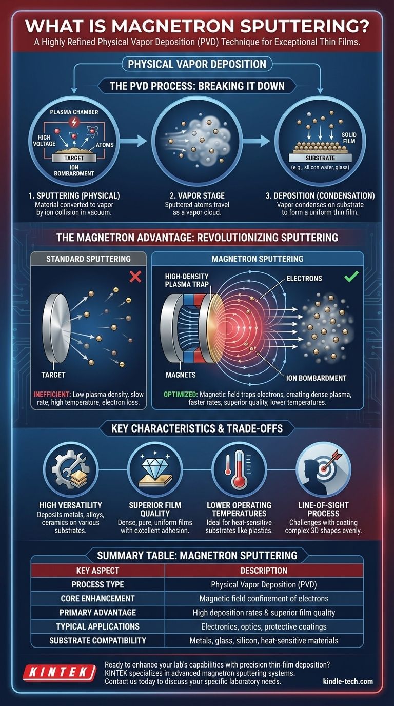
Simply put, magnetron sputtering is a type of Physical Vapor Deposition (PVD). It is a highly refined vacuum-coating technique used to deposit exceptionally thin films of virtually any material onto a surface, or substrate. As a magnetically enhanced evolution of older sputtering methods, it leverages a plasma and a magnetic field to physically eject atoms from a source material and deposit them as a high-quality coating.
The core principle to understand is that magnetron sputtering isn't just a deposition method; it's an optimization. By adding a magnetic field to a standard sputtering process, it dramatically increases the efficiency of creating a plasma, leading to faster, denser, and more uniform coatings at lower temperatures.
Deconstructing the "Physical Vapor Deposition" Process
To understand magnetron sputtering, we first need to break down the fundamental process of PVD it belongs to. The name itself describes the sequence: a material is converted into a vapor by physical means, which then condenses onto a substrate as a solid film.
The Core Concept: Sputtering
Sputtering is a physical, not chemical, process. Imagine it as a form of nanoscale sandblasting.
Inside a vacuum chamber, a high voltage is applied, and an inert gas like Argon is introduced. This creates a plasma—an energized state of matter containing positive ions and free electrons.
These positive ions are accelerated by the electric field and forcefully collide with a source material, known as the target. The sheer kinetic energy of these collisions is enough to knock off, or "sputter," individual atoms from the target's surface.
The "Vapor" and "Deposition" Stages
The ejected atoms travel through the low-pressure vacuum chamber. This cloud of sputtered atoms acts as a vapor.
When these vaporized atoms reach the substrate (the object being coated, like a silicon wafer or piece of glass), they land and condense back into a solid state, gradually building up a thin, uniform film.
The "Magnetron" Advantage: How Magnets Revolutionize Sputtering
Standard sputtering works, but it can be slow and inefficient. Magnetron sputtering introduces a crucial enhancement—a magnetic field—that dramatically improves the process's speed and quality.
The Problem with Basic Sputtering
In a simple sputtering system, many of the free electrons generated in the plasma are lost before they can ionize the Argon gas. This means you need relatively high gas pressures to achieve a sputtering rate that is useful, and the process remains inefficient.
Introducing the Magnetic Field
In magnetron sputtering, powerful magnets are placed behind the target material. This creates a magnetic field that is orthogonal (perpendicular) to the electric field on the surface of the target.
This magnetic field has a profound effect on the light, negatively charged electrons, but a much smaller effect on the heavy, positive Argon ions.
Creating a High-Density Plasma Trap
The magnetic field traps the highly mobile electrons, forcing them into a spiral path near the target's surface. This creates a dense, localized cloud of electrons.
Because these electrons are confined to the target area instead of escaping, they are far more likely to collide with and ionize the neutral Argon gas atoms. This creates a cascade effect, generating a much denser and more sustainable plasma right where it's needed most.
The Result: Faster and Better Deposition
This magnetically confined, high-density plasma dramatically increases the number of Argon ions being created.
More ions mean a more intense bombardment of the target, leading to a much higher sputtering rate. This directly translates to a faster deposition rate on the substrate, making the entire process more efficient for industrial applications.
Key Characteristics and Trade-offs
Magnetron sputtering is widely used because its advantages align perfectly with the demands of modern manufacturing, but it's important to understand its characteristics.
Benefit: High Versatility
This technique is remarkably flexible. It can be used to deposit thin films of almost any material, including metals, alloys, ceramics, and even some insulating materials, onto a wide range of substrates.
Benefit: Superior Film Quality
The films produced are known for being extremely dense, pure, and uniform. They also demonstrate excellent adhesion to the substrate, which is critical for performance in electronics, optics, and protective coatings.
Benefit: Lower Operating Temperatures
Because the magnetic field makes the process so efficient, it can be run at lower pressures and overall temperatures. This is a critical advantage for coating heat-sensitive substrates, such as plastics or other organic materials, without causing damage.
Consideration: It's a Line-of-Sight Process
Like spraying paint from a can, sputtering is a "line-of-sight" technique. The sputtered material travels in a relatively straight line from the target to the substrate. This can make it challenging to evenly coat complex, three-dimensional objects without sophisticated substrate rotation and manipulation.
Making the Right Choice for Your Goal
Understanding the nature of magnetron sputtering helps you determine if it's the right choice for a specific application.
- If your primary focus is speed and manufacturing throughput: Magnetron sputtering is a high-rate deposition method ideal for industrial-scale production where efficiency is paramount.
- If your primary focus is material quality and performance: The process creates dense, uniform films with excellent adhesion, making it a superior choice for high-performance applications in optics and semiconductors.
- If your primary focus is coating delicate or heat-sensitive substrates: Its ability to operate at lower temperatures makes it one of the best methods for depositing high-quality films onto plastics and other materials that cannot withstand high heat.
By intelligently applying a magnetic field, magnetron sputtering transforms a basic physical process into a highly controllable and efficient manufacturing technique for advanced materials.
Summary Table:
| Key Aspect | Description |
|---|---|
| Process Type | Physical Vapor Deposition (PVD) |
| Core Enhancement | Magnetic field confinement of electrons |
| Primary Advantage | High deposition rates & superior film quality |
| Typical Applications | Electronics, optics, protective coatings |
| Substrate Compatibility | Metals, glass, silicon, heat-sensitive materials |
Ready to enhance your lab's capabilities with precision thin-film deposition?
KINTEK specializes in advanced lab equipment and consumables, including magnetron sputtering systems designed for superior film quality and efficiency. Whether you're in R&D or production, our solutions help you achieve dense, uniform coatings on a wide range of substrates.
Contact us today to discuss how our expertise can support your specific laboratory needs and drive your projects forward.
Visual Guide