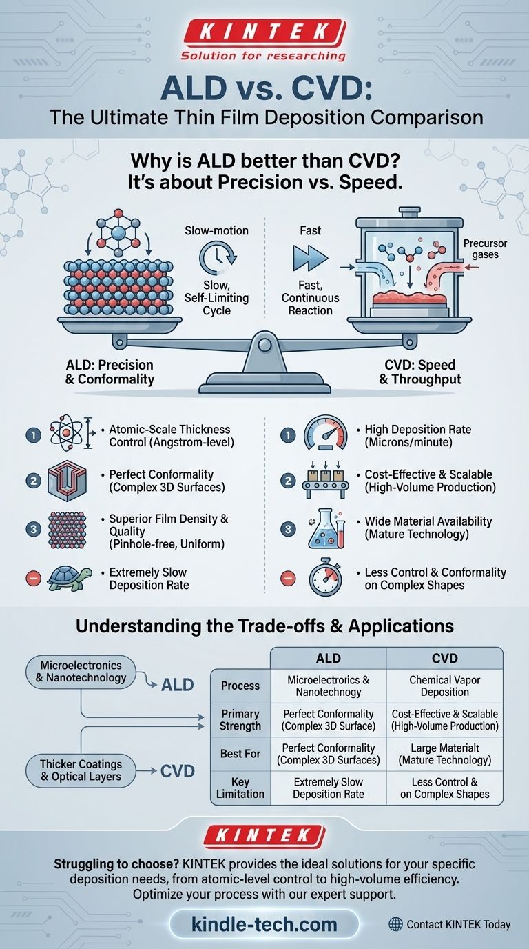
To be precise, Atomic Layer Deposition (ALD) is considered "better" than Chemical Vapor Deposition (CVD) when the primary goal is achieving unparalleled control over film thickness, density, and uniformity, especially on complex, three-dimensional surfaces. This superiority comes from its unique, self-limiting, layer-by-layer deposition process. However, this precision comes at the cost of speed, making CVD the superior choice for applications demanding high-volume, rapid deposition of thicker films.
The choice between ALD and CVD is not about which is universally better, but rather a fundamental trade-off between precision and speed. ALD offers atomic-level control, while CVD offers manufacturing efficiency and high deposition rates.
The Fundamental Difference: Process Control
The distinct advantages and disadvantages of ALD and CVD stem directly from their core operational mechanisms.
How CVD Works: A Continuous Reaction
In Chemical Vapor Deposition (CVD), gaseous precursor chemicals are introduced into a reaction chamber simultaneously.
They react together on and near the heated substrate surface, leading to a continuous and rapid deposition of the desired film. This process is efficient but less controlled.
How ALD Works: A Self-Limiting Cycle
Atomic Layer Deposition (ALD) breaks the deposition process into a sequence of separate, self-limiting steps.
First, one precursor gas is pulsed into the chamber, forming a single, stable atomic layer (a monolayer) on the substrate. Any excess gas is purged. Then, a second precursor is introduced, reacting only with the first layer. This cycle is repeated to build the film one atomic layer at a time, giving it its name.
Where ALD Excels: Unmatched Precision and Conformality
The cyclical, self-limiting nature of ALD provides capabilities that are simply not possible with the continuous process of CVD.
Atomic-Scale Thickness Control
Because ALD deposits a predictable amount of material with each cycle (ideally, one atomic layer), the final film thickness is a simple function of the number of cycles performed.
This allows for the creation of films with angstrom-level precision, which is critical for modern semiconductor manufacturing and nanotechnology.
Perfect Conformality
Conformality is the ability of a film to coat a textured or complex surface uniformly. ALD is unmatched in this regard.
The self-limiting reactions ensure the film grows evenly across every exposed surface, including deep trenches and complex 3D structures with very high aspect ratios. CVD often struggles here, producing thicker films at the top of a feature and thinner films at the bottom.
Superior Film Density and Quality
The slow, controlled, layer-by-layer growth of ALD typically results in films that are incredibly dense, pinhole-free, and highly uniform.
This methodical process minimizes the incorporation of impurities and structural defects that can occur in the faster, more chaotic CVD environment.
Understanding the Trade-offs: Why CVD is Still Essential
While ALD's precision is remarkable, it has significant limitations that ensure CVD remains a vital industrial process. The idea that ALD is simply "better" overlooks these critical factors.
The Need for Speed: Deposition Rate
The primary drawback of ALD is its extremely slow deposition rate. Building a film one atomic layer at a time is a meticulous and time-consuming process.
CVD is orders of magnitude faster, making it the only practical choice for applications requiring thick films (measured in microns rather than nanometers).
Cost, Throughput, and Scalability
The slowness of ALD directly translates to lower manufacturing throughput and, consequently, higher costs per substrate.
For applications where atomic-level precision is unnecessary, CVD offers a far more economical and scalable solution for mass production.
Material and Precursor Availability
CVD is a more mature technology with a vast library of well-documented processes for a wider range of materials.
While ALD is rapidly expanding, finding suitable, self-limiting chemical precursors for novel materials can still be a significant research and development challenge.
Making the Right Choice for Your Application
The decision to use ALD or CVD should be driven entirely by your project's specific technical and economic requirements.
- If your primary focus is cutting-edge microelectronics or nanotechnology: Choose ALD for its atomic-level precision and perfect conformality on complex 3D structures.
- If your primary focus is high-volume production of thicker protective or optical coatings: Choose CVD for its superior deposition speed, lower cost, and high throughput.
- If your primary focus is creating an ultra-dense, defect-free barrier layer: Lean towards ALD, as its controlled process minimizes impurities and ensures complete coverage.
Ultimately, selecting the right method requires matching the unique strengths of each deposition process to your specific engineering goals.
Summary Table:
| Feature | Atomic Layer Deposition (ALD) | Chemical Vapor Deposition (CVD) |
|---|---|---|
| Process | Cyclical, self-limiting, layer-by-layer | Continuous, simultaneous precursor reaction |
| Primary Strength | Atomic-scale thickness control, perfect conformality | High deposition rate, high throughput |
| Best For | Ultra-thin, uniform films on complex 3D structures (e.g., semiconductors) | Thicker coatings, high-volume production |
| Key Limitation | Very slow deposition speed | Less precise control on complex geometries |
Struggling to choose the right deposition method for your project? The experts at KINTEK understand that the decision between ALD's precision and CVD's speed is critical for your lab's success. We specialize in providing the ideal lab equipment and consumables to meet your specific thin film deposition needs, whether you require atomic-level control or high-volume efficiency.
Let us help you optimize your process and achieve superior results. Contact KINTEK today for a personalized consultation and discover how our solutions can enhance your research or production workflow.
Visual Guide