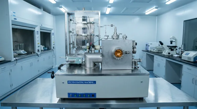
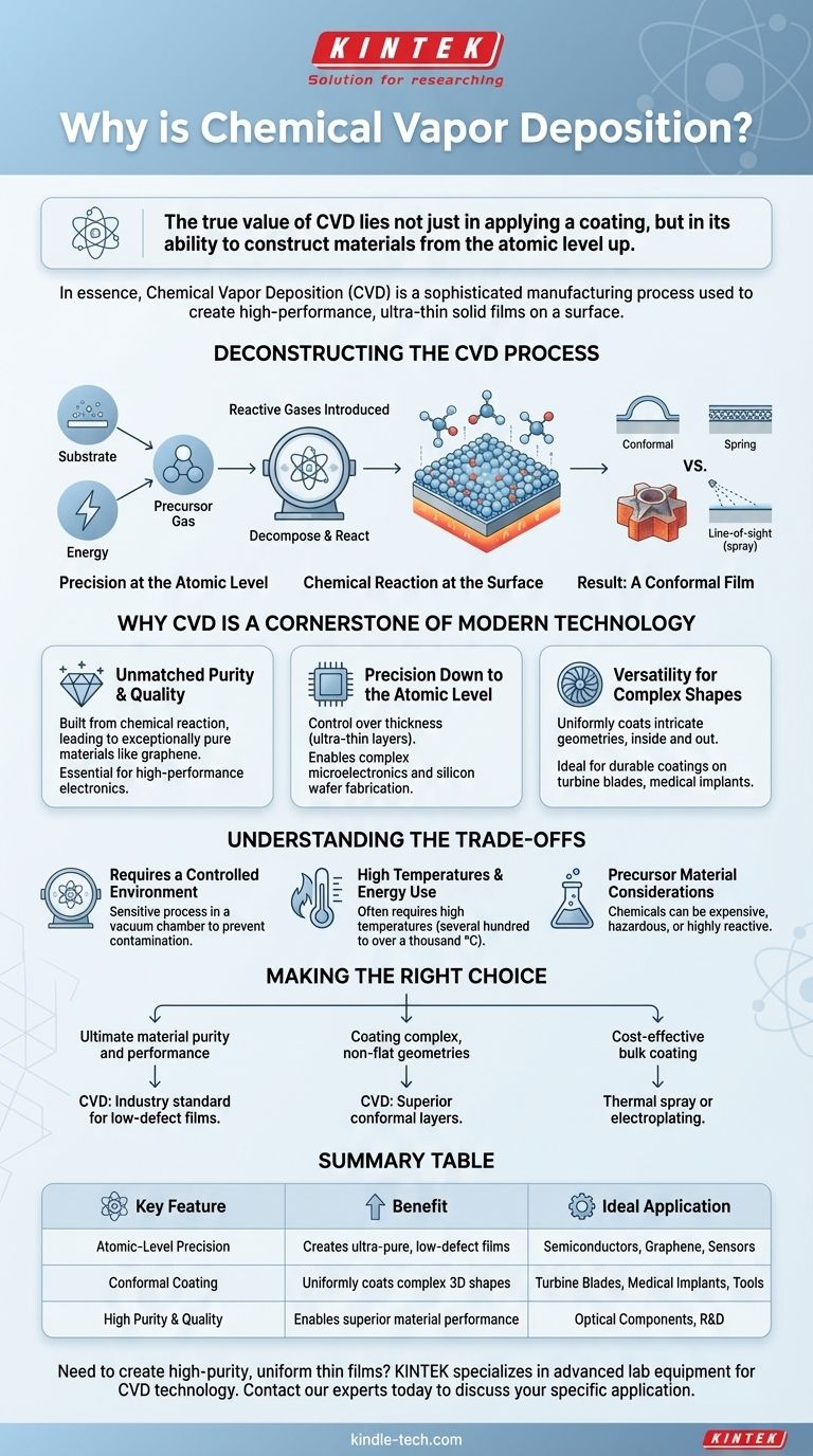
In essence, Chemical Vapor Deposition (CVD) is a sophisticated manufacturing process used to create high-performance, ultra-thin solid films on a surface. It works by introducing reactive gases (precursors) into a chamber, which then decompose and react on a heated object (substrate), building up the desired material layer by layer with exceptional purity and control.
The true value of CVD lies not just in applying a coating, but in its ability to construct materials from the atomic level up. This precision enables the creation of next-generation electronics, durable components, and advanced materials that would be impossible to produce with conventional methods.
Deconstructing the CVD Process
To understand why CVD is so powerful, we must first look at its fundamental mechanics. It is less like painting a surface and more like precisely constructing a crystal structure on it.
The Core Components
The process relies on three key elements: a substrate (the object to be coated), a precursor gas (the source material), and energy (typically heat). The substrate is placed inside a vacuum chamber.
Volatile precursor gases, which contain the atoms needed for the final film, are then introduced into the chamber.
The Chemical Reaction at the Surface
Once the precursor gas molecules come into contact with the heated substrate, a series of events is triggered. The thermal energy causes the gas molecules to react or decompose.
This chemical reaction deposits the desired solid material directly onto the substrate's surface, while any unwanted byproducts are removed as gas.
The Result: A Conformal Film
Over time, this process builds a thin, dense, and highly pure film. Because the precursor is a gas, it flows around and into every feature of the substrate, ensuring an incredibly uniform coating. This is known as a conformal coating.
This differs fundamentally from "line-of-sight" processes like spray painting, which cannot evenly coat complex or internal surfaces.
Why CVD is a Cornerstone of Modern Technology
The unique nature of the CVD process gives it capabilities that are critical for manufacturing the most advanced products. Its importance stems from delivering a combination of purity, precision, and versatility that other processes cannot match.
Unmatched Purity and Quality
Because the film is built directly from a chemical reaction using pure gases, the resulting material can be exceptionally pure and have a near-perfect structure.
This is why CVD is a leading method for producing graphene and other advanced semiconductors. The low defect count is essential for high-performance electronics where even tiny impurities can cause failure.
Precision Down to the Atomic Level
CVD allows for a very high degree of control over the thickness and properties of the deposited film. It is possible to create ultra-thin layers, sometimes just a few atoms thick.
This level of precision is the bedrock of modern microelectronics, enabling the fabrication of complex electrical circuits and processors on silicon wafers.
Versatility for Complex Shapes
The non-line-of-sight nature of the process means CVD can uniformly coat intricate and complex geometries, both inside and out.
This is invaluable for creating durable, protective coatings on components like turbine blades, medical implants, or industrial tools, where complete and even coverage is critical for performance and longevity.
Understanding the Trade-offs
While powerful, CVD is not a universal solution. Its precision comes with specific requirements and limitations that make it unsuitable for certain applications.
Requires a Controlled Environment
CVD processes are sensitive and must occur within a vacuum chamber. This is necessary to prevent contamination from air and to control the reaction chemistry precisely.
This requirement increases the complexity and cost of the equipment compared to simpler coating methods performed at atmospheric pressure.
High Temperatures and Energy Use
Most CVD processes rely on high temperatures (often several hundred to over a thousand degrees Celsius) to drive the chemical reactions.
This high energy consumption can be a significant operational cost. Furthermore, the substrate material must be able to withstand these temperatures without being damaged or melting.
Precursor Material Considerations
The choice of precursor chemicals is critical. They can be expensive, hazardous, or highly reactive, requiring specialized handling and safety protocols. The chemistry must be perfectly matched to the desired film and substrate.
Making the Right Choice for Your Goal
Deciding if CVD is the appropriate technology depends entirely on your end goal, balancing the need for ultimate performance against cost and complexity.
- If your primary focus is ultimate material purity and performance: CVD is the industry standard for creating the low-defect, high-purity films required for advanced semiconductors, sensors, and optical components.
- If your primary focus is coating complex, non-flat geometries: CVD's ability to create perfectly conformal layers on intricate surfaces makes it superior to any line-of-sight deposition technique.
- If your primary focus is cost-effective bulk coating: For thick, non-critical coatings on simple shapes, faster and less expensive methods like thermal spray or electroplating may be more appropriate.
Ultimately, chemical vapor deposition is the enabling technology for applications where material perfection and atomic-scale control are non-negotiable.
Summary Table:
| Key Feature | Benefit | Ideal Application |
|---|---|---|
| Atomic-Level Precision | Creates ultra-pure, low-defect films | Semiconductors, Graphene, Sensors |
| Conformal Coating | Uniformly coats complex 3D shapes | Turbine Blades, Medical Implants, Tools |
| High Purity & Quality | Enables superior material performance | Optical Components, R&D |
Need to create high-purity, uniform thin films for your laboratory or production line? KINTEK specializes in providing advanced lab equipment and consumables for precise material deposition. Our expertise in CVD technology can help you achieve the material perfection your project demands. Contact our experts today to discuss your specific application and discover the right solution for your laboratory needs.
Visual Guide
Related Products
- Chemical Vapor Deposition CVD Equipment System Chamber Slide PECVD Tube Furnace with Liquid Gasifier PECVD Machine
- Customer Made Versatile CVD Tube Furnace Chemical Vapor Deposition Chamber System Equipment
- Microwave Plasma Chemical Vapor Deposition MPCVD Machine System Reactor for Lab and Diamond Growth
- 915MHz MPCVD Diamond Machine Microwave Plasma Chemical Vapor Deposition System Reactor
- Custom CVD Diamond Coating for Lab Applications
People Also Ask
- What types of substrates are used in CVD to facilitate graphene films? Optimize Graphene Growth with the Right Catalyst
- What happens during deposition chemistry? Building Thin Films from Gaseous Precursors
- How expensive is chemical vapor deposition? Understanding the True Cost of High-Performance Coating
- What are the core advantages of PE-CVD in OLED encapsulation? Protect Sensitive Layers with Low-Temp Film Deposition
- What is plasma enhanced chemical vapor deposition PECVD equipment? A Guide to Low-Temperature Thin Film Deposition


