Deposition uniformity is the foundational metric that determines whether a semiconductor device will function correctly and whether it can be manufactured reliably. It is critical because variations in film thickness directly alter the electrical properties of active components, such as gate oxides, and cause significant failures in downstream processing steps like etching.
Uniformity is not merely a quality check; it is a structural prerequisite for process integration. Poor uniformity compromises the electrical integrity of critical layers and disrupts the timing mechanics of subsequent manufacturing steps.
The Direct Impact on Device Performance
Critical Active Layers
Films that actively participate in the operation of a device demand the highest level of precision. Components such as gate oxides or capacitor layers rely on specific thicknesses to maintain consistent capacitance and voltage handling.
If the uniformity of these layers varies, the electrical characteristics of the device become unpredictable. This leads to performance variability across the wafer, potentially rendering chips unusable.
Non-Critical Layer Tolerances
Not all films require the same stringency. Layers that serve passive roles, such as encapsulation layers, generally possess wider process windows.
While these layers are less sensitive to minor thickness variations, understanding the distinction allows manufacturers to prioritize resources where they matter most.
Manufacturing and Process Integration
The Ripple Effect on Production
A lack of uniformity in the deposition phase does not exist in isolation; it negatively impacts the steps that follow. The most significant conflict occurs during the etching process.
Etching Challenges
Etch processes are timed based on a specific film thickness. If a film has poor thickness uniformity, the etch time required for the thickest areas will differ from that of the thinnest areas.
This creates a dilemma: etching long enough to clear the thick spots may damage the underlying substrate in the thin spots. Conversely, stopping early to protect the thin spots leaves residual material in the thick areas, leading to electrical shorts or open circuits.
Understanding the Trade-offs
Balancing Precision and Efficiency
While high uniformity is generally desirable, achieving perfection across every layer can be inefficient. Striving for extremely tight specifications on non-critical films often incurs unnecessary costs and reduces throughput without adding value to the final product.
The Risk of Over-Specification
Engineers must identify which layers truly drive yield. Over-engineering the uniformity of an encapsulation layer diverts focus from critical active layers where thickness variation is a genuine failure mode.
Optimizing Your Uniformity Strategy
To ensure high yield and reliable performance, you must align your uniformity specifications with the specific function of the film.
- If your primary focus is critical device operation: Prioritize tight uniformity controls for gate oxides and capacitor layers to ensure consistent electrical behavior.
- If your primary focus is process integration: Ensure sufficient thickness uniformity to prevent under-etching or over-etching during the subsequent patterning steps.
True process control comes from understanding which variations your device can tolerate and which will break your manufacturing flow.
Summary Table:
| Factor | Impact on Manufacturing | Consequence of Poor Uniformity |
|---|---|---|
| Electrical Properties | Affects gate oxides & capacitors | Unpredictable voltage & performance failure |
| Etching Process | Disrupts timed etch cycles | Over-etching damage or residual material shorts |
| Process Integration | Influences downstream compatibility | Increased defects and reduced wafer yield |
| Cost Management | Resource allocation strategy | Over-specification leads to reduced throughput |
Elevate Your Thin-Film Precision with KINTEK
Achieving the perfect balance of deposition uniformity and process efficiency is essential for high-yield semiconductor manufacturing. At KINTEK, we understand that whether you are developing critical gate oxides or robust encapsulation layers, the right equipment makes all the difference.
From high-performance CVD and PECVD systems to our advanced high-temperature furnaces and vacuum solutions, KINTEK provides the specialized tools needed to ensure consistent film thickness and superior electrical integrity. Our comprehensive portfolio—including MPCVD systems, crushing and milling equipment, and precision hydraulic presses—is designed to support researchers and manufacturers in the most demanding laboratory and production environments.
Ready to optimize your manufacturing flow and reduce failure modes? Contact KINTEK today to discuss your equipment needs and technical specifications.
Related Products
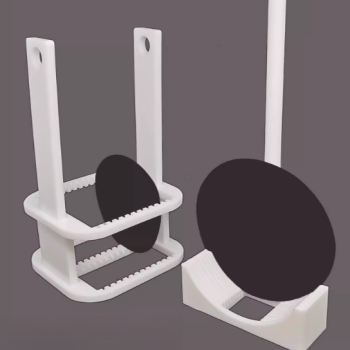
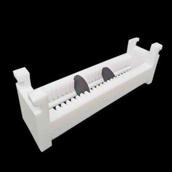
- Custom PTFE Wafer Holders for Lab and Semiconductor Processing
- CVD Diamond Dressing Tools for Precision Applications
- Chemical Vapor Deposition CVD Equipment System Chamber Slide PECVD Tube Furnace with Liquid Gasifier PECVD Machine
- Electron Beam Evaporation Coating Oxygen-Free Copper Crucible and Evaporation Boat
- RF PECVD System Radio Frequency Plasma-Enhanced Chemical Vapor Deposition RF PECVD
People Also Ask
- Why is it necessary to utilize PTFE sample holders in electroless nickel plating? Ensure Process Integrity
- Why is a custom PTFE sample holder necessary for CBD of Cd(1-x)ZnxS thin films? Ensure High Purity and Uniformity
- Why use high-quality PTFE containers for CO2 reduction electrolytes? Eliminate silicon contamination and ensure data.
- Why are PTFE containers required for PCT leaching tests? Ensure Chemical Inertness and Analytical Precision
- How does a custom PTFE electrode holder contribute to the accuracy of immersion tests? Ensure Precise Steel Analysis