Knowledge Why is thin film thickness important? The Key to Controlling Optical, Electrical, and Mechanical Properties
Author avatar

Tech Team · Kintek Solution

Updated 4 days ago

Why is thin film thickness important? The Key to Controlling Optical, Electrical, and Mechanical Properties

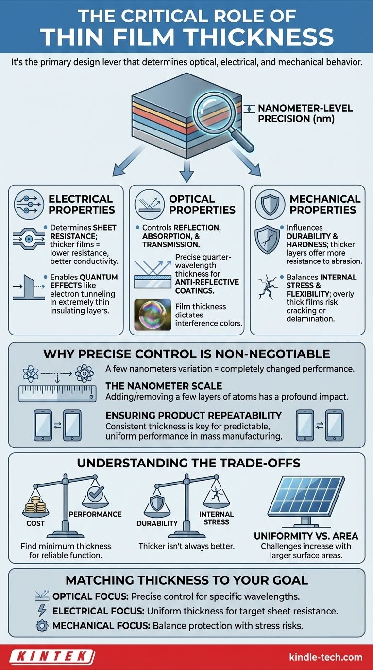
To put it simply, the thickness of a thin film is the single most critical parameter that dictates its physical properties and, therefore, its function. It is not merely a measurement but the primary design lever that determines a film's optical, electrical, and mechanical behavior. Even a variation of a few nanometers can completely change how the material performs in an application.

The core reason thin film thickness is important is that it directly correlates to function. Changing the thickness fundamentally changes how the film interacts with light, electricity, and physical stress, making precise control essential for creating reliable and effective devices.

The Direct Link Between Thickness and Function

A thin film is a layer of material ranging from a few atoms to several micrometers thick. At this microscopic scale, the physical dimension of thickness is not just a passive attribute; it actively governs the material's properties.

Electrical Properties

For conductive films, thickness is directly related to sheet resistance. A thicker film provides a larger cross-sectional area for electrons to flow, resulting in lower resistance and better conductivity.

Conversely, in semiconductor devices, some functions rely on films being extremely thin. A thin insulating layer may be required to allow a quantum mechanical effect known as electron tunneling, which would be impossible if the film were too thick.

Optical Properties

Thickness is paramount for any optical application. It determines how a film reflects, absorbs, and transmits light.

For an anti-reflective coating, the ideal thickness is precisely one-quarter of the wavelength of the light it's designed to counteract. This causes destructive interference, canceling out reflections. Any deviation from this exact thickness degrades performance.

The iridescent colors seen on soap bubbles or oil slicks are also a direct result of thin film interference, where the film's thickness determines which colors are reflected toward your eye.

Mechanical Properties

The thickness of a protective coating determines its durability and hardness. A thicker layer of a hard material like diamond-like carbon (DLC) will offer more resistance to scratches and abrasion.

However, thickness also influences internal stress and flexibility. A very thick film may be more prone to cracking or delamination, while a thinner film will be more flexible and better able to conform to a non-rigid substrate.

Why Precise Control is Non-Negotiable

Because properties are so tightly coupled to thickness, the ability to deposit a film with nanometer-level precision and repeatability is what separates a functional device from a failed one.

The Scale of Nanometers

A nanometer is one-billionth of a meter. At this scale, adding or removing just a few layers of atoms can have a profound impact on the film's overall performance.

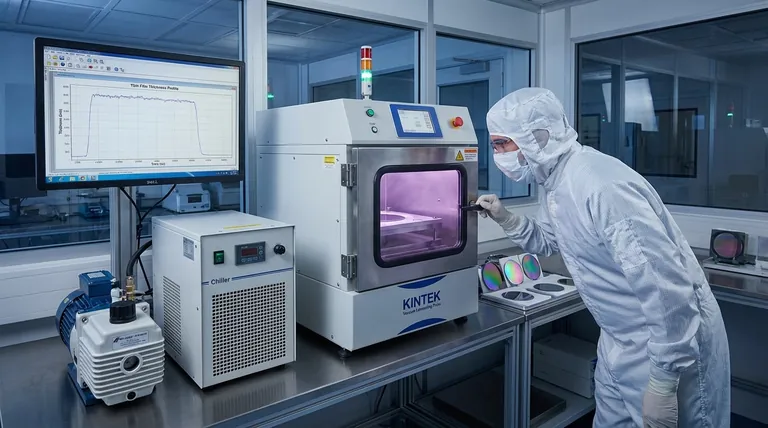
This is why deposition processes, such as sputtering, are controlled so carefully. The process is often run at a constant rate for a specific amount of time to achieve the desired thickness down to the angstrom level (one-tenth of a nanometer).

Ensuring Product Repeatability

For any commercial product, from a smartphone screen to a solar panel, every unit must perform identically. Controlling film thickness is the key to ensuring that the optical and electrical properties are consistent across millions of devices.

Without this control, device performance would be unpredictable, rendering mass manufacturing impossible.

Understanding the Trade-offs

Choosing the right film thickness is rarely about maximizing a single property. It almost always involves balancing competing requirements.

Cost vs. Performance

Depositing a thicker film takes more time and consumes more material, which directly increases manufacturing costs. The engineering goal is often to find the minimum thickness that reliably delivers the required performance, optimizing for both function and cost-effectiveness.

Durability vs. Internal Stress

While a thicker protective coating is generally more durable, it also builds up more internal stress during deposition. This stress can cause the film to crack or peel away from the substrate, especially if the substrate flexes or experiences temperature changes.

Uniformity vs. Area

Achieving a perfectly uniform thickness becomes significantly more challenging as the surface area of the substrate increases. A process that works for a small computer chip may not be suitable for coating a large architectural glass panel without introducing unacceptable thickness variations.

Matching Thickness to Your Goal

The "correct" thickness is entirely dependent on the intended application. Your primary objective should guide your material and process decisions.

  • If your primary focus is optical performance: Your thickness must be precisely controlled relative to the specific wavelengths of light you need to manage.
  • If your primary focus is electrical conductivity: You must deposit a film thick and uniform enough to meet your target for sheet resistance without adding unnecessary cost.
  • If your primary focus is mechanical protection: You must balance the need for a durable, thick coating with the risks of internal stress and potential cracking.

Ultimately, thin film thickness is the fundamental variable that translates a material's potential into predictable, real-world performance.

Summary Table:

Property How Thickness Affects It Key Consideration
Electrical Determines sheet resistance and enables quantum effects like tunneling. Critical for semiconductor and conductive film performance.
Optical Controls reflection, absorption, and transmission of light. Must be precise to the nanometer for anti-reflective coatings.
Mechanical Influences durability, hardness, flexibility, and internal stress. A balance between protection and risk of cracking/delamination.

Need precise thin film deposition for your lab's research or product development?

At KINTEK, we specialize in providing high-quality lab equipment, including sputtering systems and deposition tools, that deliver the nanometer-level thickness control essential for reliable optical, electrical, and mechanical performance. Our solutions help researchers and manufacturers achieve consistent, repeatable results, ensuring your devices function as intended.

Contact our experts today to discuss your specific thin film application and find the perfect equipment for your laboratory needs.

Related Products

People Also Ask

Related Products

RF PECVD System Radio Frequency Plasma-Enhanced Chemical Vapor Deposition RF PECVD

RF PECVD System Radio Frequency Plasma-Enhanced Chemical Vapor Deposition RF PECVD

RF-PECVD is an acronym for "Radio Frequency Plasma-Enhanced Chemical Vapor Deposition." It deposits DLC (Diamond-like carbon film) on germanium and silicon substrates. It is utilized in the 3-12um infrared wavelength range.

Inclined Rotary Plasma Enhanced Chemical Vapor Deposition PECVD Equipment Tube Furnace Machine

Inclined Rotary Plasma Enhanced Chemical Vapor Deposition PECVD Equipment Tube Furnace Machine

Upgrade your coating process with PECVD coating equipment. Ideal for LED, power semiconductors, MEMS and more. Deposits high-quality solid films at low temps.

Chemical Vapor Deposition CVD Equipment System Chamber Slide PECVD Tube Furnace with Liquid Gasifier PECVD Machine

Chemical Vapor Deposition CVD Equipment System Chamber Slide PECVD Tube Furnace with Liquid Gasifier PECVD Machine

KT-PE12 Slide PECVD System: Wide power range, programmable temp control, fast heating/cooling with sliding system, MFC mass flow control & vacuum pump.

HFCVD Machine System Equipment for Drawing Die Nano-Diamond Coating

HFCVD Machine System Equipment for Drawing Die Nano-Diamond Coating

The nano-diamond composite coating drawing die uses cemented carbide (WC-Co) as the substrate, and uses the chemical vapor phase method ( CVD method for short ) to coat the conventional diamond and nano-diamond composite coating on the surface of the inner hole of the mold.

915MHz MPCVD Diamond Machine Microwave Plasma Chemical Vapor Deposition System Reactor

915MHz MPCVD Diamond Machine Microwave Plasma Chemical Vapor Deposition System Reactor

915MHz MPCVD Diamond Machine and its multi-crystal effective growth, the maximum area can reach 8 inches, the maximum effective growth area of single crystal can reach 5 inches. This equipment is mainly used for the production of large-size polycrystalline diamond films, the growth of long single crystal diamonds, the low-temperature growth of high-quality graphene, and other materials that require energy provided by microwave plasma for growth.

Customer Made Versatile CVD Tube Furnace Chemical Vapor Deposition Chamber System Equipment

Customer Made Versatile CVD Tube Furnace Chemical Vapor Deposition Chamber System Equipment

Get your exclusive CVD furnace with KT-CTF16 Customer Made Versatile Furnace. Customizable sliding, rotating, and tilting functions for precise reactions. Order now!

CVD Diamond Domes for Industrial and Scientific Applications

CVD Diamond Domes for Industrial and Scientific Applications

Discover CVD diamond domes, the ultimate solution for high-performance loudspeakers. Made with DC Arc Plasma Jet technology, these domes deliver exceptional sound quality, durability, and power handling.

Split Chamber CVD Tube Furnace with Vacuum Station Chemical Vapor Deposition System Equipment Machine

Split Chamber CVD Tube Furnace with Vacuum Station Chemical Vapor Deposition System Equipment Machine

Efficient split chamber CVD furnace with vacuum station for intuitive sample checking and quick cooling. Up to 1200℃ max temperature with accurate MFC mass flowmeter control.

Custom PTFE Teflon Parts Manufacturer for Magnetic Stirring Bar

Custom PTFE Teflon Parts Manufacturer for Magnetic Stirring Bar

The PTFE magnetic stirring bar, made from high-quality PTFE, offers exceptional resistance to acids, alkalis, and organic solvents, coupled with high-temperature stability and low friction. Ideal for laboratory use, these stirring bars are compatible with standard flask ports, ensuring stability and safety during operations.

Custom Machined and Molded PTFE Teflon Parts Manufacturer for Laboratory ITO FTO Conductive Glass Cleaning Flower Basket

Custom Machined and Molded PTFE Teflon Parts Manufacturer for Laboratory ITO FTO Conductive Glass Cleaning Flower Basket

PTFE cleaning racks are mainly made of tetrafluoroethylene. PTFE, known as the "King of Plastics", is a polymer compound made of tetrafluoroethylene.

VHP Sterilization Equipment Hydrogen Peroxide H2O2 Space Sterilizer

VHP Sterilization Equipment Hydrogen Peroxide H2O2 Space Sterilizer

A hydrogen peroxide space sterilizer is a device that uses vaporized hydrogen peroxide to decontaminate enclosed spaces. It kills microorganisms by damaging their cellular components and genetic material.

Custom PTFE Teflon Parts Manufacturer Corrosion Resistant Cleaning Rack Flower Basket

Custom PTFE Teflon Parts Manufacturer Corrosion Resistant Cleaning Rack Flower Basket

The PTFE cleaning rack, also known as the PTFE flower basket cleaning flower basket, is a specialized laboratory tool designed for the efficient cleaning of PTFE materials. This cleaning rack ensures thorough and safe cleaning of PTFE items, maintaining their integrity and performance in laboratory settings.

High Performance Laboratory Freeze Dryer

High Performance Laboratory Freeze Dryer

Advanced lab freeze dryer for lyophilization, preserving biological & chemical samples efficiently. Ideal for biopharma, food, and research.

Multi-Punch Rotary Tablet Press Mold Ring for Rotating Oval and Square Molds

Multi-Punch Rotary Tablet Press Mold Ring for Rotating Oval and Square Molds

The multi-punch rotary tablet press mold stands as a pivotal component in pharmaceutical and manufacturing industries, revolutionizing the process of tablet production. This intricate mold system comprises multiple punches and dies arranged in a circular fashion, facilitating rapid and efficient tablet formation.

1200℃ Split Tube Furnace with Quartz Tube Laboratory Tubular Furnace

1200℃ Split Tube Furnace with Quartz Tube Laboratory Tubular Furnace

KT-TF12 split tube furnace: high-purity insulation, embedded heating wire coils, and max. 1200C. Widely used for new materials and chemical vapour deposition.

High Performance Laboratory Freeze Dryer for Research and Development

High Performance Laboratory Freeze Dryer for Research and Development

Advanced laboratory freeze dryer for lyophilization, preserving sensitive samples with precision. Ideal for biopharmaceuticals, research & food industries.

Assemble Lab Cylindrical Press Mold

Assemble Lab Cylindrical Press Mold

Get reliable and precise molding with Assemble Lab Cylindrical Press Mold. Perfect for ultra-fine powder or delicate samples, widely used in material research and development.

High-Purity Titanium Foil and Sheet for Industrial Applications

High-Purity Titanium Foil and Sheet for Industrial Applications

Titanium is chemically stable, with a density of 4.51g/cm3, which is higher than aluminum and lower than steel, copper, and nickel, but its specific strength ranks first among metals.


Leave Your Message