Lab Materials
Aluminum Boride (AlB2) Sputtering Target / Powder / Wire / Block / Granule
Item Number : LM-AlB2
Price varies based on specs and customizations
- Chemical Formula
- AlB2
- Purity
- 2N5
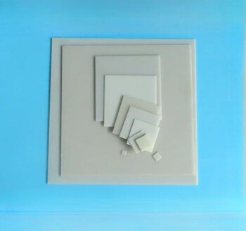
- Shape
- discs / wire / block / powder / plates / column targets / step target / custom-made

Shipping:
Contact us to get shipping details Enjoy On-time Dispatch Guarantee.
We provide Aluminum Boride (AlB2) materials for laboratory usage at reasonable prices, tailored to your unique requirements. Our expertise lies in producing Aluminum Boride (AlB2) materials of various purities, shapes, and sizes.
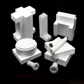
Our selection includes sputtering targets (circular, square, tubular, irregular), coating materials, cylinders, cones, particles, foils, powders, 3D printing powders, nanometer powders, wire rods, ingots, and blocks in a range of specifications and sizes.
Details

About Aluminum Boride (AlB2)
Aluminum Boride (Aluminum Diboride) is a high-melting material with metal-like conductivity, and is available in most volumes including high purity, submicron, and nanopowder forms. Borides are stable to nonoxidizing acids but breakdown in strong oxidizing agents and alkalis. They are used in semiconductors, superconductors, diamagnetic, paramagnetic, ferromagnetic, anti-ferromagnetic, turbine blades, and rocket nozzles.
Recent studies have discovered that Borides are superconductive and ultra-incompressible. We offer many standard grades, including Mil Spec (military grade); ACS, Reagent and Technical Grade; Food, Agricultural and Pharmaceutical Grade; Optical Grade, USP and EP/BP (European Pharmacopoeia/British Pharmacopoeia), and follow applicable ASTM testing standards.
We provide typical and custom packaging, as well as additional technical and safety (MSDS) data.
Ingredient Quality Control
- Raw material composition analysis
- Through the use of equipment such as ICP and GDMS, the content of metal impurities is detected and analyzed to ensure that it meets the purity standard;
Non-metallic impurities are detected by equipment such as carbon and sulfur analyzers, nitrogen and oxygen analyzers. - Metallographic flaw detection analysis
- The target material is inspected using flaw detection equipment to ensure that there are no defects or shrinkage holes inside the product;
Through metallographic testing, the internal grain structure of the target material is analyzed to ensure that the grains are fine and dense. - Appearance and dimension inspection
- Product dimensions are measured using micrometers and precision calipers to ensure compliance with drawings;
The surface finish and cleanliness of the product are measured using a surface cleanliness meter.
Conventional Sputtering Target Sizes
- Preparation process
- hot isostatic pressing, vacuum melting, etc.
- Sputtering target shape
- plane sputtering target, multi-arc sputtering target, step sputtering target, special-shaped sputtering target
- Round sputtering target size
- Diameter: 25.4mm / 50mm / 50.8mm / 60mm / 76.2mm / 80mm / 100mm / 101.6mm / 152.4mm
Thickness: 3mm / 4mm / 5mm / 6mm / 6.35mm
Size can be customized. - Square sputtering target size
- 50×50×3mm / 100×100×4mm / 300×300×5mm, size can be customized
Available Metal Forms
Metal Forms Details
We manufacture almost all the metals listed on the periodic table in a wide range of forms and purities, as well as standard sizes and dimensions. We can also produce custom-made products to meet specific customer requirements, such as size, shape, surface area, composition, and more. The following list provides a sample of the forms we offer, but it is not exhaustive. If you need laboratory consumables, please contact us directly to request a quote.
- Flat/Planar Forms: Board, Film, Foil, Microfoil, Microleaf, Paper, Plate, Ribbon, Sheet, Strip, Tape, Wafer
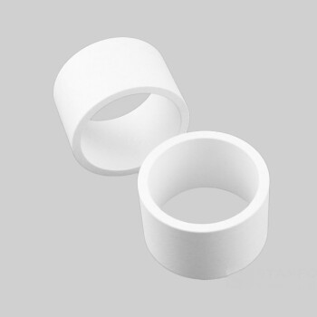
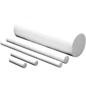
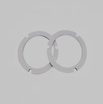
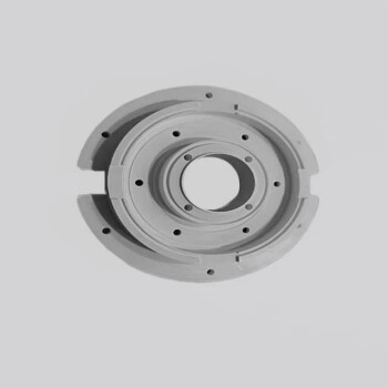
- Preformed Shapes: Anodes, Balls, Bands, Bars, Boats, Bolts, Briquettes, Cathodes, Circles, Coils, Crucibles, Crystals, Cubes, Cups, Cylinders, Discs, Electrodes, Fibers, Filaments, Flanges, Grids, Lenses, Mandrels, Nuts, Parts, Prisms, Pucks, Rings, Rods, Shapes, Shields, Sleeves, Springs, Squares, Sputtering Targets, Sticks, Tubes, Washers, Windows, Wires
- Microsizes: Beads, Bits, Capsules, Chips, Coins, Dust, Flakes, Grains, Granules, Micropowder, Needles, Particles, Pebbles, Pellets, Pins, Pills, Powder, Shavings, Shot, Slugs, Spheres, Tablets
- Macrosizes: Billets, Chunks, Cuttings, Fragments, Ingots, Lumps, Nuggets, Pieces, Punchings, Rocks, Scraps, Segments, Turnings
- Porous and Semi-Porous: Fabric, Foam, Gauze, Honeycomb, Mesh, Sponge, Wool
- Nanoscale: Nanoparticles, Nanopowders, Nanofoils, Nanotubes, Nanorods, Nanoprisms
- Others: Concentrate, Ink, Paste, Precipitate, Residue, Samples, Specimens
KinTek specializes in the manufacturing of high-purity and ultra-high-purity materials with a purity range of 99.999% (5N), 99.9999% (6N), 99.99995% (6N5), and in some cases, up to 99.99999% (7N). Our materials are available in specific grades, including UP/UHP, semiconductor, electronic, deposition, fiber optic, and MBE grades. Our high-purity metals, oxides, and compounds are specifically crafted to meet the rigorous demands of high-technology applications and are ideal for use as dopants and precursor materials for thin film deposition, crystal growth of semiconductors, and synthesis of nanomaterials. These materials find use in advanced microelectronics, solar cells, fuel cells, optical materials, and other cutting-edge applications.
Packaging
We use vacuum packaging for our high-purity materials, and each material has specific packaging tailored to its unique characteristics. For instance, our Hf sputter target is externally tagged and labeled to facilitate efficient identification and quality control. We take great care to prevent any damage that could occur during storage or transportation.
4.8
out of
5
KINTEK's Aluminum Boride (AlB2) materials are of exceptional quality, ensuring precise thin film deposition. The rotating target design enables faster deposition and greater surface coverage.
4.7
out of
5
I'm consistently impressed with KINTEK's Aluminum Boride (AlB2) materials. Their custom design target requests accommodate our unique needs, resulting in tailored solutions that enhance our research outcomes.
4.9
out of
5
The Aluminum Boride (AlB2) materials from KINTEK have proven to be highly durable, withstanding the rigors of our demanding experimental conditions. Their resilience ensures consistent performance over extended periods.
4.6
out of
5
KINTEK's Aluminum Boride (AlB2) materials are remarkably versatile, enabling a wide range of applications in our laboratory. Their adaptability has facilitated groundbreaking research and innovative discoveries.
4.8
out of
5
The Aluminum Boride (AlB2) materials from KINTEK are a game-changer in our lab. Their exceptional purity and well-defined properties have significantly enhanced the accuracy and reliability of our experimental results.
4.7
out of
5
KINTEK's Aluminum Boride (AlB2) materials have revolutionized our research capabilities. Their advanced technological features have enabled us to explore new avenues of scientific inquiry and achieve groundbreaking results.
4.9
out of
5
The Aluminum Boride (AlB2) materials from KINTEK are an invaluable asset to our laboratory. Their consistent quality and exceptional performance have contributed significantly to our research success.
4.6
out of
5
KINTEK's Aluminum Boride (AlB2) materials have exceeded our expectations. Their customizable options and tailored solutions have empowered us to optimize our research processes and achieve remarkable outcomes.
4.8
out of
5
The Aluminum Boride (AlB2) materials from KINTEK are a testament to their commitment to innovation. Their cutting-edge technology has opened up new possibilities for our research, enabling us to delve deeper into complex scientific mysteries.
4.7
out of
5
KINTEK's Aluminum Boride (AlB2) materials have been instrumental in our groundbreaking research. Their reliability and consistency have allowed us to replicate experiments with precision, leading to significant scientific advancements.
4.9
out of
5
The Aluminum Boride (AlB2) materials from KINTEK are a true marvel of scientific engineering. Their exceptional properties have enabled us to achieve unprecedented levels of accuracy and efficiency in our research endeavors.
4.6
out of
5
KINTEK's Aluminum Boride (AlB2) materials have transformed our laboratory into a hub of innovation. Their versatility and adaptability have empowered us to tackle complex challenges and uncover hidden truths in the world of science.
4.8
out of
5
The Aluminum Boride (AlB2) materials from KINTEK are a testament to their dedication to scientific excellence. Their unwavering commitment to quality has been instrumental in our groundbreaking discoveries.
4.7
out of
5
KINTEK's Aluminum Boride (AlB2) materials have been a game-changer for our research. Their exceptional performance and reliability have enabled us to push the boundaries of scientific knowledge and make significant contributions to our field.
4.9
out of
5
The Aluminum Boride (AlB2) materials from KINTEK are a true asset to our laboratory. Their consistent quality and exceptional properties have been instrumental in our successful research outcomes and groundbreaking discoveries.
4.6
out of
5
KINTEK's Aluminum Boride (AlB2) materials have revolutionized the way we conduct research. Their innovative features and tailored solutions have empowered us to explore new avenues of scientific inquiry and achieve remarkable breakthroughs.
4.8
out of
5
The Aluminum Boride (AlB2) materials from KINTEK are a testament to their commitment to scientific advancement. Their cutting-edge technology has enabled us to unlock new possibilities in our research and make significant contributions to the scientific community.
4.7
out of
5
KINTEK's Aluminum Boride (AlB2) materials have been a game-changer for our laboratory. Their exceptional quality and reliability have enabled us to achieve groundbreaking results and make significant contributions to our field of study.
4.9
out of
5
The Aluminum Boride (AlB2) materials from KINTEK are a true testament to their dedication to scientific excellence. Their unwavering commitment to innovation has been instrumental in our groundbreaking discoveries and has pushed the boundaries of scientific knowledge.
REQUEST A QUOTE
Our professional team will reply to you within one business day. Please feel free to contact us!
Related Products
High Purity Aluminum Oxide (Al2O3) Sputtering Target / Powder / Wire / Block / Granule
Looking for Aluminum Oxide materials for your lab? We offer high-quality Al2O3 products at affordable prices with customizable shapes and sizes to meet your specific needs. Find sputtering targets, coating materials, powders, and more.
High Purity Aluminum (Al) Sputtering Target / Powder / Wire / Block / Granule
Get high-quality Aluminum (Al) materials for laboratory use at affordable prices. We offer customized solutions including sputtering targets, powders, foils, ingots & more to meet your unique needs. Order now!
Nickel Aluminum Alloy (NiAl) Sputtering Target / Powder / Wire / Block / Granule
Looking for high-quality Nickel Aluminum Alloy materials for your lab? Our experts produce and customize NiAl materials to suit your specific needs. Find a wide range of sizes and specifications for sputtering targets, coating materials, and more at affordable prices.
Boron Carbide (BC) Sputtering Target / Powder / Wire / Block / Granule
Get high-quality Boron Carbide materials at reasonable prices for your lab needs. We customize BC materials of different purities, shapes, and sizes, including sputtering targets, coatings, powders, and more.
Lithium Aluminum Alloy (AlLi) Sputtering Target / Powder / Wire / Block / Granule
Looking for Lithium Aluminum Alloy materials for your lab? Our expertly produced and tailored AlLi materials come in various purities, shapes, and sizes, including sputtering targets, coatings, powders, and more. Get reasonable prices and unique solutions today.
High Purity Boron (B) Sputtering Target / Powder / Wire / Block / Granule
Get affordable Boron (B) materials tailored to your specific lab needs. Our products range from sputtering targets to 3D printing powders, cylinders, particles, and more. Contact us today.
Aluminum Copper Alloy (AlCu) Sputtering Target / Powder / Wire / Block / Granule
Get high-quality Aluminum Copper Alloy (AlCu) materials for your laboratory needs at affordable prices. Customized purities, shapes, and sizes available. Shop sputtering targets, coating materials, powders, and more.
Aluminum Nitride (AlN) Sputtering Target / Powder / Wire / Block / Granule
High-quality Aluminum Nitride (AlN) materials in various shapes and sizes for laboratory use at affordable prices. Explore our range of sputtering targets, coatings, powders, and more. Customized solutions available.
Boron Nitride (BN) Ceramics-Conductive Composite
Due to the characteristics of boron nitride itself, the dielectric constant and dielectric loss are very small, so it is an ideal electrical insulating material.

Boron Nitride (BN) Ceramic Plate
Boron nitride (BN) ceramic plates do not use aluminum water to wet, and can provide comprehensive protection for the surface of materials that directly contact molten aluminum, magnesium, zinc alloys and their slag.
Boron Nitride (BN) Sputtering Target / Powder / Wire / Block / Granule
Shop Boron Nitride materials for your laboratory needs at reasonable prices. We tailor materials to your requirements with varying purities, shapes, and sizes. Choose from a wide range of specifications and sizes.
Boron Nitride (BN) Ceramic Parts
Boron nitride ((BN) is a compound with high melting point, high hardness, high thermal conductivity and high electrical resistivity. Its crystal structure is similar to graphene and harder than diamond.
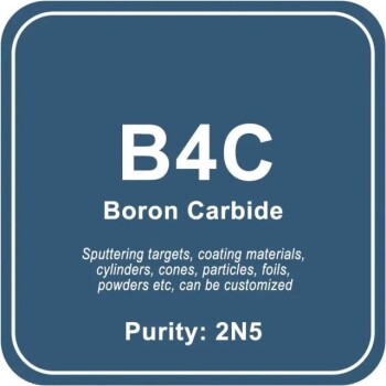
Boron Carbide (B4C) Sputtering Target / Powder / Wire / Block / Granule
Get high-quality Boron Carbide (B4C) materials for your laboratory needs at affordable prices. We offer tailored materials of different purities, shapes, and sizes to suit your unique requirements, including sputtering targets, coatings, particles, and more.
Boron Nitride (BN) Ceramic Tube
Boron nitride (BN) is known for its high thermal stability, excellent electrical insulating properties and lubricating properties.
Boron Nitride (BN) Ceramic Rod
Boron nitride (BN) rod is the strongest boron nitride crystal form like graphite, which has excellent electrical insulation, chemical stability and dielectric properties.
Hexagonal Boron Nitride (HBN) Ceramic Ring
Boron nitride ceramic (BN) rings are commonly used in high temperature applications such as furnace fixtures, heat exchangers and semiconductor processing.
High Purity Cobalt (Co) Sputtering Target / Powder / Wire / Block / Granule
Get affordable Cobalt (Co) materials for laboratory use, tailored to your unique needs. Our range includes sputtering targets, powders, foils, and more. Contact us today for customized solutions!
Boron Nitride (BN) Ceramic Custom Parts
Boron nitride (BN) ceramics can have different shapes, so they can be manufactured to generate high temperature, high pressure, insulation and heat dissipation to avoid neutron radiation.
Nickel Niobium Alloy (NiNb) Sputtering Target / Powder / Wire / Block / Granule
Find high-quality Nickel Niobium Alloy (NiNb) materials for your laboratory needs. We offer tailored purities, shapes, and sizes, plus sputtering targets, coatings, powders, and more. Explore our range now!

Electron Beam Evaporation Coating Conductive Boron Nitride Crucible (BN Crucible)
High-purity and smooth conductive boron nitride crucible for electron beam evaporation coating, with high temperature and thermal cycling performance.
Aluminum Nitride (AlN) Ceramic Sheet
Aluminum nitride (AlN) has the characteristics of good compatibility with silicon. It is not only used as a sintering aid or reinforcing phase for structural ceramics, but its performance far exceeds that of alumina.
Alkali-free / Boro-aluminosilicate glass
Boroaluminosilicate glass is highly resistant to thermal expansion, making it suitable for applications that require resistance to temperature changes, such as laboratory glassware and cooking utensils.