Introduction to CVD Technology
Definition and Importance
Chemical Vapor Deposition (CVD) stands as a pivotal thin film deposition technology, playing a crucial role in semiconductor manufacturing and a myriad of other industries. This technology enables the precise and controlled deposition of thin films onto various substrates, which is essential for the fabrication of electronic components, optical coatings, and protective layers.
In semiconductor manufacturing, CVD is indispensable for creating high-quality, uniform films that enhance the performance and reliability of integrated circuits. The ability to deposit materials with specific properties, such as conductivity, insulation, and optical transparency, makes CVD an essential tool in the production of advanced microelectronic devices.
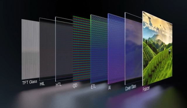
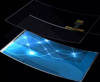
Beyond semiconductors, CVD finds extensive applications in display technology, where it is used to deposit indium tin oxide (ITO) films and copper films, enhancing the functionality and durability of display devices. Additionally, CVD is utilized in the production of optical coatings for lenses and mirrors, as well as in anti-corrosion coatings for metal surfaces, demonstrating its versatility across diverse fields.
The significance of CVD lies not only in its wide-ranging applications but also in its ability to produce films with exceptional uniformity, adhesion, and controllability. These attributes make CVD an indispensable technology for advancing various industries and driving innovation in materials science.
Working Principle of CVD
Chemical Reaction Process
During the Chemical Vapor Deposition (CVD) process, the formation of thin films relies on a controlled chemical reaction. Initially, gas precursors, which are the raw materials for the desired film, are introduced into the reaction chamber. These precursors are typically volatile compounds that can be easily vaporized. Once inside the chamber, these gases are subjected to heat, often in the range of several hundred to thousands of degrees Celsius, depending on the specific precursor and desired film properties.
The heating process is crucial as it provides the energy necessary for the gas molecules to overcome their activation energy barriers, enabling them to react. As the temperature rises, the gas precursors decompose and react with each other or with the surface of the substrate. This reaction typically occurs at the substrate surface, where the precursors adsorb and then undergo further decomposition or combination. The resulting products from these reactions include the desired film material, which deposits onto the substrate, and by-products, which are usually gaseous and are exhausted from the system.
For instance, in the deposition of silicon films, a common precursor is silane (SiH4). When heated, silane decomposes into silicon and hydrogen gas. The silicon atoms then deposit onto the substrate, forming a continuous film, while the hydrogen gas is evacuated from the reaction chamber. This example illustrates the dynamic nature of the CVD process, where precise control over temperature and precursor flow rates is essential to achieve the desired film quality and uniformity.
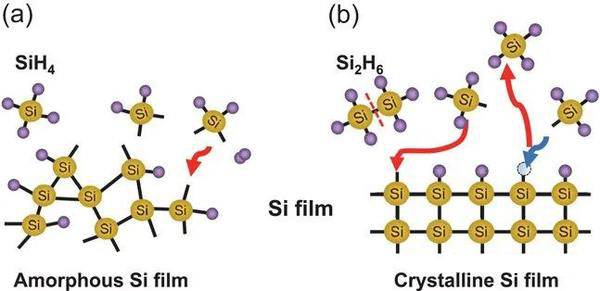
The chemical reaction process in CVD is not limited to simple decompositions; it can also involve complex reactions such as oxidation, nitridation, or the formation of compound materials. These reactions are often facilitated by the presence of additional reactant gases, such as oxygen or nitrogen, which are introduced into the chamber to modify the film properties. For example, when depositing silicon dioxide (SiO2) films, silane is reacted with oxygen to form the oxide layer.
Example Reaction
In the context of Chemical Vapor Deposition (CVD), one of the primary reactions involves the decomposition of trichlorosilane (SiHCl₃). This process is fundamental to the formation of thin films, particularly in semiconductor manufacturing. When SiHCl₃ is heated, it undergoes a complex chemical transformation. The silicon source material, SiHCl₃, breaks down into elemental silicon, which then deposits onto the substrate. Simultaneously, chlorine (Cl₂) and hydrochloric acid (HCl) gases are liberated as byproducts. These gases are typically exhausted from the reaction chamber, ensuring that they do not interfere with the deposition process.
This reaction exemplifies the core principle of CVD, where precursor gases are converted into solid films through controlled chemical reactions. The decomposition of SiHCl₃ not only provides the necessary silicon for film formation but also illustrates the importance of gas management in maintaining a clean and efficient deposition environment. The byproduct gases, Cl₂ and HCl, are crucial to monitor and control, as their presence can affect the quality and uniformity of the deposited film.
Classification of CVD
Thermal CVD
Thermal Chemical Vapor Deposition (CVD) involves heating precursor gases to a high temperature, typically above 700°C, within a reaction chamber. This elevated temperature is crucial for promoting the decomposition of the precursor gases, which then deposit onto the substrate to form a thin film. The process relies on the thermal energy to drive the chemical reactions necessary for film formation, ensuring that the deposited film exhibits enhanced properties such as improved crystallinity, greater density, and faster deposition rates.
In thermal CVD, the gaseous reactants are often carried into the reactor chamber by an inert gas like nitrogen, which helps in maintaining a controlled environment. The high temperatures not only facilitate the decomposition of the precursors but also enable reactions that would otherwise be impossible at lower temperatures. However, these high temperatures can lead to drawbacks such as stress formation within the film, higher diffusion rates of elements from the substrate into the film, and potential degradation of the substrate itself.
| Advantages | Disadvantages |
|---|---|
| Enhanced deposition rate | Stress formation |
| Improved crystallinity | Higher diffusion rates |
| Greater film density | Substrate degradation |
Thermal CVD is particularly advantageous in semiconductor manufacturing, where it is used to deposit thin films such as silicon dioxide, silicon nitride, and polysilicon on silicon wafers. These films are essential for the fabrication of integrated circuits and other electronic devices. Despite its advantages, thermal CVD requires careful management of temperature and precursor delivery rates to optimize the deposition process and mitigate potential drawbacks.
Plasma Enhanced CVD (PECVD)
Plasma Enhanced Chemical Vapor Deposition (PECVD) is a specialized variant of Chemical Vapor Deposition (CVD) that leverages plasma to augment the reaction rate and meticulously control the deposition process. Unlike traditional CVD methods, which rely solely on thermal energy to decompose precursor gases, PECVD employs plasma to activate the reactive gases, thereby facilitating the deposition at significantly lower temperatures, typically ranging between 100 and 600 °C.
In PECVD, the plasma acts as a catalyst, breaking down the reactive precursors into their constituent atoms or molecules, which then react and deposit on the substrate surface. This plasma-assisted breakdown allows for the deposition of various films, including silicon (Si), silicon dioxide (SiO2), silicon nitride, silicon oxynitride, and silicon carbide, at temperatures as low as 200-350 °C. This lower temperature range is particularly advantageous for applications involving temperature-sensitive materials, such as aluminum, where higher temperatures could compromise the integrity of the substrate.
The PECVD process is often carried out in a parallel plate, capacitively coupled plasma system. In this setup, the substrate is positioned on a grounded electrode, while the plasma is generated between two electrodes. The gases used in PECVD can vary depending on the desired film properties, with common gases including silane (SiH4), nitrous oxide (N2O), ammonia (NH3), helium (He), argon (Ar), nitrogen trifluoride (NF3), and phosphine (PH3). Each gas plays a specific role in the deposition process, contributing to the formation of the desired film.
One of the key technical specifications of PECVD is its ability to operate at temperatures below 540 °C, making it suitable for a wide range of substrates. The process chamber is typically equipped with multiple gas chambers, such as silane chambers (A + C) and a TEOS (Tetraethyl Orthosilicate) chamber (B), each designed to handle different gas mixtures and deposition requirements. This modular design allows for greater flexibility and control over the deposition process, ensuring the production of high-quality films with precise properties.
Metal Organic CVD (MOCVD)
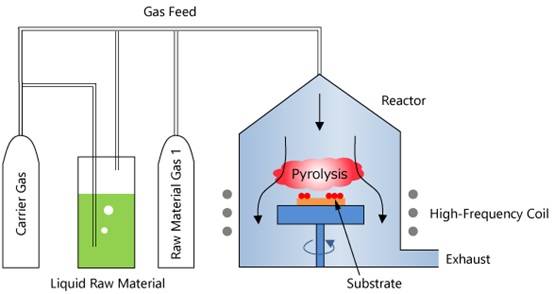
Metal Organic Chemical Vapor Deposition (MOCVD) is an advanced epitaxial growth technique that utilizes metal organic compounds as precursor gases for the deposition of metal and semiconductor films. This method is particularly notable for its ability to grow a wide range of compound semiconductors, including Ⅲ-V and Ⅱ-VI materials, as well as their multilayered solid solutions.
Key Features of MOCVD
-
Source Materials: MOCVD employs organic compounds of group III and II elements, along with hydrides of group V and VI elements, as the primary source materials for crystal growth. These materials are introduced into the reaction chamber in gaseous form, where they undergo thermal decomposition to form thin, single-crystal layers on the substrate.
-
Precision Control: One of the significant advantages of MOCVD is the precise control over the composition and dopant concentration of the deposited films. This precision is achieved by regulating the flow rate and on/off timing of the gaseous precursors, allowing for the growth of thin and ultra-thin layer materials with high accuracy.
-
Rapid Switching: The relatively fast gas flow rate within the reaction chamber enables quick changes in the composition and dopant concentration of the multiple compounds. This rapid switching capability reduces the likelihood of memory effects, facilitating the creation of steep interfaces and making MOCVD ideal for the growth of heterostructures, superlattices, and quantum well materials.
Advantages Over Other Epitaxial Techniques
Compared to other epitaxial growth methods, MOCVD offers several distinct advantages:
| Advantage | Description |
|---|---|
| Component Control | The gaseous state of the precursors allows for precise control over the components, dopant concentration, and thickness of the epitaxial layer. |
| Rapid Adjustments | Quick changes in gas flow rates enable rapid adjustments in compound composition, reducing memory effects and enhancing interface quality. |
| Versatility | Suitable for a wide range of compound semiconductors, including Ⅲ-V and Ⅱ-VI materials, making it highly versatile for various applications. |
Applications of CVD
Semiconductor Manufacturing
In semiconductor manufacturing, Chemical Vapor Deposition (CVD) plays a pivotal role in creating advanced materials that enhance device performance and reliability. The process involves the deposition of various films, including silicides, nitride films, and metal films, each tailored for specific applications within the semiconductor industry.
Silicides
Silicides, formed by the reaction of silicon with metals, are crucial for reducing contact resistance and improving the efficiency of semiconductor devices. They are commonly used in gate electrodes, interconnects, and contact pads. For instance, tungsten silicide (WSi₂) is often employed in CMOS technology due to its low resistivity and thermal stability.
Nitride Films
Nitride films, such as silicon nitride (Si₃N₄), serve multiple purposes in semiconductor manufacturing. They act as diffusion barriers, preventing the migration of dopants and impurities, and as passivation layers, protecting the device from environmental factors. Additionally, nitride films are integral to the formation of capacitors in DRAM devices, ensuring high capacitance and low leakage currents.
Metal Films
Metal films, including aluminum (Al) and copper (Cu), are essential for creating interconnects that facilitate the flow of electrical signals within integrated circuits. Copper, in particular, is favored for its low resistivity and ability to reduce power consumption and heat generation. The use of CVD in depositing these metal films ensures uniform coverage and excellent adhesion, critical for maintaining the integrity and performance of semiconductor devices.
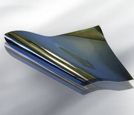
By leveraging CVD technology, semiconductor manufacturers can achieve precise control over the deposition process, resulting in high-quality films that meet the stringent requirements of modern electronic devices.
Display Technology
In the realm of display technology, Indium Tin Oxide (ITO) films and copper films play pivotal roles. These materials are integral to the fabrication of various display devices, enhancing their performance and functionality.
Indium Tin Oxide (ITO) Films
ITO films are renowned for their exceptional electrical conductivity and optical transparency. This unique combination makes them ideal for applications such as:
- Touch Screens: Providing the conductive layer necessary for touch-sensitive displays.
- Electroluminescent Panels: Facilitating the emission of light in displays.
- Solar Cells: Enhancing the efficiency of photovoltaic devices by allowing light to pass through while conducting electricity.
Copper Films
Copper films, on the other hand, are celebrated for their high electrical conductivity and mechanical strength. These properties are leveraged in:
- Flexible Displays: Offering durability and efficient signal transmission.
- High-Resolution Displays: Ensuring minimal signal loss and high-speed data processing.
- Advanced Packaging: Supporting the interconnectivity in complex electronic systems.
Both ITO and copper films are typically deposited using Chemical Vapor Deposition (CVD) techniques, which allow for precise control over film thickness and uniformity, ensuring optimal performance in display devices.
Other Fields
Chemical Vapor Deposition (CVD) technology extends its applications beyond semiconductor manufacturing and display technology, penetrating into diverse industries that require precise and durable coatings. One prominent application is in optical coatings, where CVD is employed to deposit thin films on lenses, mirrors, and other optical components. These coatings enhance light transmission, reduce reflection, and improve overall optical performance, making them indispensable in fields such as telecommunications, aerospace, and medical imaging.
Another significant application is in anti-corrosion coatings. CVD techniques are used to create protective layers on metals and alloys, shielding them from harsh environmental conditions and prolonging their service life. This is particularly crucial in industries like automotive, aerospace, and marine engineering, where materials are exposed to corrosive elements.
| Application | Industry Impact |
|---|---|
| Optical Coatings | Enhances optical devices, crucial for telecommunications and medical imaging. |
| Anti-corrosion Coatings | Protects metals in automotive, aerospace, and marine sectors, extending lifespan. |
These applications underscore the versatility and robustness of CVD technology, making it a cornerstone in modern industrial processes.
CVD Process Characteristics
High Temperature Requirement
The high temperature requirement in the Chemical Vapor Deposition (CVD) process is pivotal for several reasons. Firstly, elevated temperatures are essential to promote the reaction speed of the precursor gases. When heated, these gases undergo decomposition and subsequent chemical reactions on the substrate surface, leading to the formation of the desired thin film. The kinetic energy provided by the heat ensures that the molecules have sufficient energy to react and form stable bonds.
Moreover, high temperatures help in enhancing the diffusion rate of the reactants on the substrate. This diffusion is crucial for achieving uniform film deposition across the surface. Without adequate heat, the diffusion process would be sluggish, resulting in non-uniform and potentially defective films.
Additionally, high temperatures play a role in removing impurities from the reaction environment. Impurities such as moisture or residual gases can be driven off at elevated temperatures, ensuring a cleaner deposition process. This purification aspect is particularly important in the manufacturing of high-purity materials used in semiconductor devices.
| Temperature Range | Effect |
|---|---|
| Low (<400°C) | Slow reaction rates, limited diffusion, potential for non-uniform films. |
| Medium (400-800°C) | Optimized for many CVD processes, balanced reaction and diffusion rates. |
| High (>800°C) | Fast reactions, high diffusion rates, but may exceed substrate thermal limits. |
Vacuum Environment
The CVD process is typically conducted under a vacuum environment. This controlled atmosphere is crucial for several reasons. Firstly, a vacuum minimizes the presence of contaminants, such as oxygen and water vapor, which could otherwise interfere with the chemical reactions and degrade the quality of the deposited film. Secondly, maintaining a vacuum helps to manage the pressure within the deposition chamber, ensuring that the gas precursors flow at optimal rates and react efficiently on the substrate surface.
In a vacuum, the mean free path of gas molecules is increased, reducing collisions between molecules. This reduction in collisions allows for more directed movement of the gas precursors towards the substrate, enhancing the deposition process. Additionally, the vacuum environment facilitates better control over the temperature and pressure conditions, which are critical parameters in the CVD process.
| Benefit | Description |
|---|---|
| Contaminant Reduction | Minimizes interference from oxygen and water vapor. |
| Pressure Management | Ensures optimal flow and reaction of gas precursors. |
| Increased Mean Free Path | Reduces molecular collisions, enhancing deposition. |
| Temperature Control | Facilitates better control over critical parameters. |
The vacuum environment is not just a technical requirement but a fundamental aspect that underpins the efficiency and precision of the CVD process. By maintaining a vacuum, manufacturers can achieve high-quality, uniform films with the desired properties, making it an indispensable part of the CVD technology.
Surface Preparation
Before any coating process, particularly in Chemical Vapor Deposition (CVD), the surface of the substrate must undergo rigorous preparation to ensure optimal adhesion and film quality. This step is crucial as it directly impacts the performance and longevity of the deposited thin films.
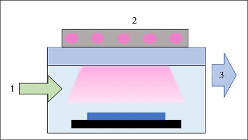
Contaminants such as organic residues, oxides, and moisture must be meticulously removed. These impurities can hinder the chemical reactions necessary for film formation and lead to defects like pinholes or non-uniform coatings. Techniques for surface preparation vary, but common methods include chemical cleaning, etching, and plasma treatment.
-
Chemical Cleaning: This involves using solvents or acids to dissolve and remove organic and inorganic contaminants. For instance, RCA cleaning is a standard method that uses a mixture of hydrogen peroxide and sulfuric acid to clean silicon wafers.
-
Etching: This method selectively removes surface layers using chemical reactions. For example, hydrofluoric acid is often used to remove native silicon dioxide from silicon substrates.
-
Plasma Treatment: This technique uses plasma to activate the surface, enhancing its reactivity and cleaning it of any residual contaminants. It is particularly effective for removing organic residues and improving surface energy.
Each of these methods plays a vital role in ensuring that the substrate is free from contaminants, thereby facilitating the successful deposition of high-quality thin films. Proper surface preparation not only enhances the adhesion of the deposited film but also ensures that the film properties, such as uniformity and density, meet the required specifications.
Substrate Limitations
Temperature and reactivity limitations are critical factors that can significantly restrict the range of applicable substrates in Chemical Vapor Deposition (CVD) processes. The high temperatures required for the chemical reactions to occur can impose thermal constraints on the substrate material, limiting the choice to those that can withstand such extreme conditions without degradation or deformation. For instance, certain organic materials or low-melting-point metals may not be suitable due to their inability to maintain structural integrity at elevated temperatures.
Moreover, the reactivity of the precursor gases and the resulting chemical interactions with the substrate surface can further narrow the selection of suitable materials. Some substrates may react unfavorably with the deposition gases, leading to undesirable side reactions or the formation of non-uniform films. This reactivity limitation necessitates careful selection and pre-treatment of substrates to ensure compatibility with the CVD process.
Coverage and Masking
In the context of Chemical Vapor Deposition (CVD), the process of coverage and masking plays a crucial role in determining the final quality and functionality of the deposited thin films. While CVD ensures that all areas of the substrate are uniformly covered with the desired material, the ability to selectively mask specific areas becomes a critical factor in achieving precise patterns and structures.
The coverage aspect of CVD is highly effective, as it typically results in a uniform deposition of material across the entire substrate surface. This uniformity is essential for applications where even film thickness is necessary, such as in semiconductor manufacturing and display technology. However, the challenge arises when specific areas of the substrate need to be protected from the deposition process. This is where masking techniques come into play.
Masking in CVD involves the use of physical barriers or photoresist layers to prevent the deposition of material in certain regions. While this technique is generally effective, it does come with limitations. For instance, the precision of the masking process can be affected by factors such as the type of substrate, the complexity of the pattern, and the specific CVD parameters used. Additionally, the masking materials themselves must be chosen carefully to ensure they do not react with the deposition gases or degrade under the high temperatures typically involved in CVD processes.
Film Thickness Limitation
The thickness of thin films deposited through Chemical Vapor Deposition (CVD) is inherently constrained by several factors, primarily the process parameters and the physical state of the materials involved. These limitations are critical to understanding the practical applications and boundaries of CVD technology.
Process Parameters
The deposition process itself imposes several constraints on film thickness. Key factors include:
- Temperature and Pressure: The high temperatures required for CVD reactions can limit the thickness of the deposited film. Extreme temperatures can cause thermal degradation or non-uniformity in the film. Similarly, the pressure under which the process is conducted can affect the film's growth rate and uniformity.
- Reaction Kinetics: The rate at which precursor gases react and form the desired film is another limiting factor. Faster reactions can lead to thinner films if the process is not carefully controlled.
Material State
The physical and chemical properties of the precursor materials also play a significant role:
- Precursor Stability: The stability of precursor gases at high temperatures can limit the thickness of the film. Unstable precursors may decompose prematurely, leading to incomplete or non-uniform films.
- Substrate Compatibility: The substrate material's ability to withstand the deposition conditions is crucial. Certain substrates may not be able to sustain the high temperatures or reactivity required for thicker film deposition.
These constraints are not merely limitations but are integral to the process, ensuring that the deposited films are of high quality and suitable for their intended applications.
Adhesion
Excellent adhesion properties are a hallmark of Chemical Vapor Deposition (CVD) technology, which is crucial for the durability and functionality of the thin films it produces. The adhesion of these films is influenced by several factors, including the surface preparation of the substrate, the chemical reactivity of the precursor gases, and the process conditions such as temperature and pressure.
For instance, proper surface preparation ensures that contaminants are removed, creating a clean and reactive surface that enhances the bonding between the film and the substrate. This step is particularly important in semiconductor manufacturing, where even minor impurities can lead to significant performance issues.
The chemical nature of the precursor gases also plays a pivotal role. The reaction between the gas precursors and the substrate surface forms a strong chemical bond, which is the basis for the excellent adhesion observed in CVD films. This chemical bonding mechanism ensures that the deposited films remain firmly attached to the substrate, even under harsh operational conditions.
Process conditions, such as the high temperatures required for CVD, further contribute to the strong adhesion. These high temperatures not only promote the chemical reactions necessary for film formation but also allow for better diffusion of the film materials into the substrate, creating a more robust interface.
Advantages of CVD Technology
Uniformity
Uniformity in Chemical Vapor Deposition (CVD) is a critical attribute that ensures consistent film quality across large area substrates. This uniformity is achieved through meticulous control of the process parameters, including temperature, pressure, and precursor flow rates. The ability to maintain uniformity is particularly crucial in semiconductor manufacturing, where even minor variations can lead to significant performance issues in the final product.
To illustrate, consider a typical CVD setup where the substrate is exposed to a uniform flow of precursor gases. The gas molecules diffuse and react on the substrate surface, forming a thin film. By precisely managing the distribution of these gases, manufacturers can ensure that the deposition occurs uniformly across the entire substrate, regardless of its size. This is often facilitated by advanced reactor designs that promote even gas distribution and minimize localized variations.
| Parameter | Impact on Uniformity |
|---|---|
| Temperature | Ensures uniform decomposition and deposition of precursors. |
| Pressure | Aids in maintaining a consistent gas flow and reaction rate. |
| Precursor Flow | Controls the concentration and distribution of reactive species. |
In summary, the uniformity in CVD processes is not merely a desirable feature but a fundamental requirement for producing high-quality thin films. It underscores the importance of precise process control and advanced reactor technology in achieving consistent results across large substrates.
Controllability
One of the standout features of Chemical Vapor Deposition (CVD) technology is its high degree of controllability over the deposition process. This controllability is essential for achieving precise film properties and deposition rates, which are critical for various applications in semiconductor manufacturing, display technology, and beyond.

Deposition Rate Control
The deposition rate in CVD can be meticulously controlled by adjusting several parameters. These include:
- Temperature: By varying the temperature of the substrate and the precursor gases, the rate at which the chemical reactions occur can be fine-tuned. Higher temperatures generally accelerate the reaction rate, leading to faster deposition.
- Pressure: Operating under different pressures can influence the flow dynamics of the precursor gases and the rate at which they reach the substrate surface.
- Gas Flow Rates: Controlling the flow rates of the precursor gases allows for precise adjustments in the concentration of reactants at the substrate, thereby affecting the deposition rate.
Film Properties Customization
Beyond just the rate of deposition, CVD offers extensive control over the properties of the resulting film. Key properties that can be customized include:
- Film Thickness: By carefully managing the process parameters, the thickness of the deposited film can be controlled within a narrow range, ensuring uniformity across large substrates.
- Chemical Composition: The use of different precursor gases or mixtures allows for the deposition of films with varying chemical compositions, tailored to specific application requirements.
- Crystal Structure: The temperature and pressure conditions can influence the crystallinity of the deposited film, enabling the creation of either amorphous or crystalline structures as needed.
- Stress: The internal stress within the film can be controlled to prevent defects and ensure the film's integrity and adhesion to the substrate.
Process Flexibility
CVD's controllability extends to the flexibility of the process itself. Different types of CVD, such as Thermal CVD, Plasma Enhanced CVD (PECVD), and Metal Organic CVD (MOCVD), offer unique advantages and control mechanisms. For instance, PECVD uses plasma to enhance the reaction rate and provide additional control over the deposition process, while MOCVD allows for the use of metal organic compounds to deposit complex materials.
Versatility
Chemical Vapor Deposition (CVD) technology stands out for its exceptional versatility, making it a cornerstone in various industries. This versatility is primarily attributed to its ability to deposit a wide array of materials, each tailored to specific applications. Whether it's creating high-quality semiconductor films, enhancing display technologies, or developing protective coatings, CVD proves its adaptability across different material types and functional requirements.
Material Diversity
CVD's capability to handle diverse materials is a significant advantage. From silicon and metal films to complex compounds like nitrides and oxides, the range of materials that can be processed is extensive. This broad spectrum ensures that CVD can meet the stringent demands of modern technological applications, from microelectronics to advanced optics.
Application Flexibility
Beyond material diversity, CVD's flexibility extends to its application in multiple fields. In semiconductor manufacturing, it is indispensable for creating silicides, nitride films, and metal layers, each playing a crucial role in device performance. In display technology, CVD is employed to deposit Indium Tin Oxide (ITO) and copper films, enhancing the functionality and durability of screens. Additionally, CVD finds utility in less conventional areas such as optical coatings and anti-corrosion treatments, further illustrating its versatility.
Process Adaptability
The adaptability of CVD processes is another facet of its versatility. Techniques like Thermal CVD, Plasma Enhanced CVD (PECVD), and Metal Organic CVD (MOCVD) each offer unique advantages, allowing for precise control over the deposition process. This adaptability ensures that CVD can be optimized for different substrates and environmental conditions, making it a versatile tool in the hands of researchers and engineers.
Related Products
- HFCVD Machine System Equipment for Drawing Die Nano-Diamond Coating
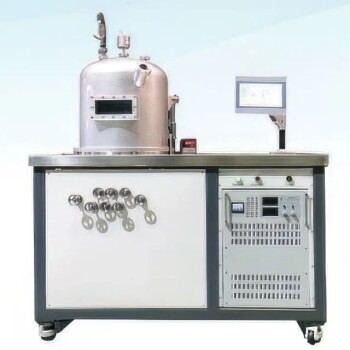
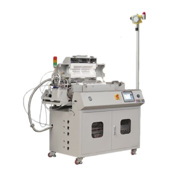
- Chemical Vapor Deposition CVD Equipment System Chamber Slide PECVD Tube Furnace with Liquid Gasifier PECVD Machine
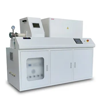
- Customer Made Versatile CVD Tube Furnace Chemical Vapor Deposition Chamber System Equipment
- 915MHz MPCVD Diamond Machine Microwave Plasma Chemical Vapor Deposition System Reactor
- Custom CVD Diamond Coating for Lab Applications
Related Articles
- Understanding the CVD Diamond Machine and How It Works
- How CVD Coating Can Help You Achieve High Purity and Density
- Comparing Chemical Vapor Deposition and Physical Vapor Deposition
- Chemical Vapor Deposition (CVD) and Electronic Specialty Gases
- In-Depth Examination of Chemical Vapor Deposition (CVD) Coatings
