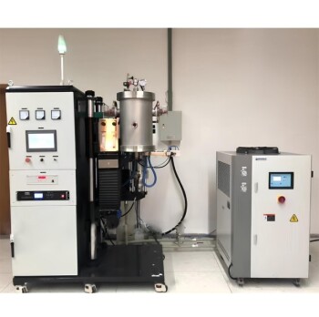
Types of Bias Power Supplies in Magnetron Sputtering
DC Constant Voltage Type
The DC constant voltage type bias power supply is specifically designed to maintain a steady output of direct current (DC) voltage, which is crucial for the sputtering of target materials. This type of power supply ensures a stable energy delivery, which is essential for the consistency and quality of the sputtered films. By providing a constant voltage, it allows for precise control over the energy applied to the target material, thereby optimizing the sputtering process.
In magnetron sputtering, where the goal is to deposit a uniform and high-quality film onto a substrate, the stability of the energy delivery is paramount. The DC constant voltage type power supply achieves this by maintaining a consistent voltage level, which helps in achieving uniform film thickness and composition. This stability is particularly important in applications where the target material requires a specific energy level to achieve the desired film properties.
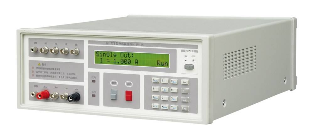
Moreover, the use of a DC constant voltage power supply in sputtering processes contributes to the overall efficiency and reliability of the system. It minimizes fluctuations in the energy delivery, which can otherwise lead to variations in the film quality. This makes the DC constant voltage type an ideal choice for applications that demand high precision and consistency in the sputtering process.
DC Constant Current Type
The DC constant current type bias power supply is specifically designed to deliver a consistent and stable direct current (DC) output, which is crucial for processes that require precise current control. This type of power supply is particularly beneficial in sputtering applications involving metal materials, where maintaining a steady current is essential for achieving uniform and high-quality film deposition.
In sputtering processes, the constant current ensures that the energy delivered to the target material remains stable, thereby preventing fluctuations that could lead to inconsistent film properties. This stability is particularly important in applications where the film thickness and uniformity are critical, such as in the production of optical coatings or electronic components.
Moreover, the DC constant current supply is adept at managing the complex interactions between the plasma and the target material, ensuring that the sputtering process remains efficient and effective. This is achieved by maintaining a consistent ion bombardment rate, which helps in achieving the desired film density and adhesion.
Pulse Type
The pulse type bias power supply is specifically designed to output voltage or current in a pulsed form, which is particularly advantageous for sputtering dielectric materials or preparing composite film layers. This type of power supply introduces intermittent energy bursts into the sputtering process, allowing for precise control over the deposition of materials with varying electrical properties.
For dielectric materials, the pulsed output helps mitigate issues such as arcing and charge accumulation, which are common challenges in traditional continuous power methods. By alternating between high-energy pulses and low-energy intervals, the pulse type power supply can effectively reduce the risk of damage to sensitive dielectric layers.
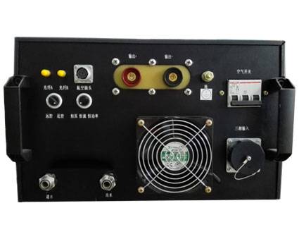
In the context of composite film layers, the pulsed output enables the deposition of multiple materials with different sputtering characteristics. This is achieved by adjusting the pulse frequency and amplitude, allowing for the creation of complex, multi-layered structures that would be difficult to achieve with a constant power supply. The ability to alternate between materials with varying sputtering rates ensures a more uniform and adherent film, enhancing the overall quality and functionality of the composite structure.
Feedback Type
In magnetron sputtering, the Feedback Type bias power supply stands out for its ability to dynamically adjust the output voltage or current through a sophisticated feedback control loop. This adaptive mechanism ensures that the sputtering process remains stable and optimized, regardless of the variations that may occur during the deposition process. The feedback control loop continuously monitors key parameters, such as the target material's condition and the plasma environment, and makes real-time adjustments to maintain the desired sputtering conditions.
This type of power supply is particularly advantageous in applications where precision and consistency are critical. For instance, when sputtering complex materials or creating multilayer films, the ability to fine-tune the output in real-time can significantly enhance the quality and uniformity of the deposited film. The feedback mechanism not only stabilizes the sputtering process but also allows for greater flexibility in handling different types of target materials and varying process conditions.
Moreover, the Feedback Type bias power supply is essential in processes where maintaining a stable plasma environment is crucial. By continuously adjusting the output, it helps to counteract any fluctuations in plasma density or energy, thereby ensuring that the sputtered particles reach the substrate with the correct energy and in a consistent manner. This is particularly important in applications requiring high-quality, defect-free films, such as in the semiconductor industry or in the production of optical coatings.
High-Power Type
The High-Power Type bias power supply is specifically designed to meet the demanding requirements of large-area or high-speed sputtering processes. This type of power supply is engineered to deliver significantly higher output power, making it an ideal choice for applications such as the preparation of large-area films or in industrial production lines where efficiency and throughput are paramount.
In large-scale manufacturing environments, the need for consistent and rapid deposition of film layers across expansive substrates is critical. The High-Power Type excels in these scenarios by providing the necessary energy to sustain high-speed sputtering operations, ensuring that the target material is effectively and uniformly distributed across the substrate surface. This results in not only faster production rates but also in the creation of high-quality, uniform films that meet stringent industrial standards.
Moreover, the high-power capabilities of this type of bias power supply are particularly advantageous in processes that require the sputtering of dense, high-quality films. The increased energy output allows for the efficient bombardment of the target material, facilitating the formation of dense, adherent films that are resistant to delamination and other common defects. This makes the High-Power Type an indispensable tool in industries where the integrity and longevity of the deposited films are critical to product performance and reliability.
Purpose of Bias Voltage in Sputtering
Enhancing Surface Preparation
The application of bias voltage in magnetron sputtering plays a critical role in enhancing the surface preparation of workpieces. By increasing the energy of charged particles within the vacuum plasma environment, the bias voltage effectively bombards the surface of the workpiece. This bombardment serves a dual purpose: it cleans the surface by removing contaminants and roughens it to create a more conducive environment for film adhesion.
The cleaning process is particularly important as it ensures that the surface is free from impurities such as oxides, hydrocarbons, and other residues that could hinder the adhesion of the film layer. The increased energy of the charged particles ensures that these contaminants are effectively dislodged and removed, leaving a clean and reactive surface.
In addition to cleaning, the bombardment induced by the bias voltage also creates a micro-rough surface. This roughness is beneficial as it increases the surface area available for adhesion, thereby improving the mechanical interlocking between the film and the substrate. This dual effect—cleaning and surface roughening—significantly enhances the overall adhesion of the film layer, ensuring a stronger and more durable bond.
The process of enhancing surface preparation through bias voltage is not only crucial for the initial stages of film deposition but also has long-term implications for the performance and longevity of the final product. By ensuring a clean and rough surface, the bias voltage sets the stage for optimal film adhesion, which is essential for applications ranging from microelectronics to industrial coatings.
Improving Film Adhesion
The application of bias voltage in magnetron sputtering plays a crucial role in improving film adhesion. This process involves increasing the energy of charged particles within the vacuum plasma environment, which subsequently enhances the interaction between the film layer and the substrate. The higher energy levels enable these charged particles to bombard the substrate surface more intensely, effectively cleaning and roughening it. This roughening creates a more textured surface, which is known to significantly improve the mechanical interlocking between the film and the substrate, thereby enhancing adhesion.
Moreover, the enhanced energy levels not only facilitate better surface preparation but also promote the formation of stronger chemical bonds between the film and the substrate. This is particularly important in cases where the substrate material and the film material have different chemical properties. By ensuring a thorough and effective surface interaction, the bias voltage ensures that the film adheres more securely, reducing the likelihood of delamination or other adhesion-related issues.
Related Products
- Reference Electrode Calomel Silver Chloride Mercury Sulfate for Laboratory Use
- Laboratory CVD Boron Doped Diamond Materials
- Microwave Plasma Chemical Vapor Deposition MPCVD Machine System Reactor for Lab and Diamond Growth
- Round Bidirectional Press Mold for Lab
- E Beam Crucibles Electron Gun Beam Crucible for Evaporation
Related Articles
- Design and Application of Reference Electrodes in Lithium Batteries
- Electrochemistry Basics: Conditions and Precautions for Using Different Reference Electrodes
- Common Reference Electrodes in Electrochemical Studies
- Comprehensive Guide to Reference Electrodes: Types, Applications, and Selection Criteria
- Reference Electrodes: Calomel, Silver Chloride, and Mercury Sulfate - A Comprehensive Guide
