Transferring graphene is a critical, multi-step procedure that bridges the gap between synthesis and application. The most common method involves using a polymer, typically Poly(methyl methacrylate) or PMMA, as a temporary support scaffold. This polymer coat allows the fragile, single-atom-thick graphene sheet to be safely lifted from its growth substrate and moved to a new, functional substrate.
The core challenge of graphene transfer is moving a microscopic, fragile film without introducing defects like tears or wrinkles. The standard solution is a "wet transfer" process that uses a sacrificial polymer layer for mechanical support while the original growth metal is chemically etched away.
Why is Graphene Transfer Necessary?
The need for a transfer process stems from how high-quality graphene is produced. The method dictates the necessity of moving the material to a useful surface.
The Problem of Growth vs. Application
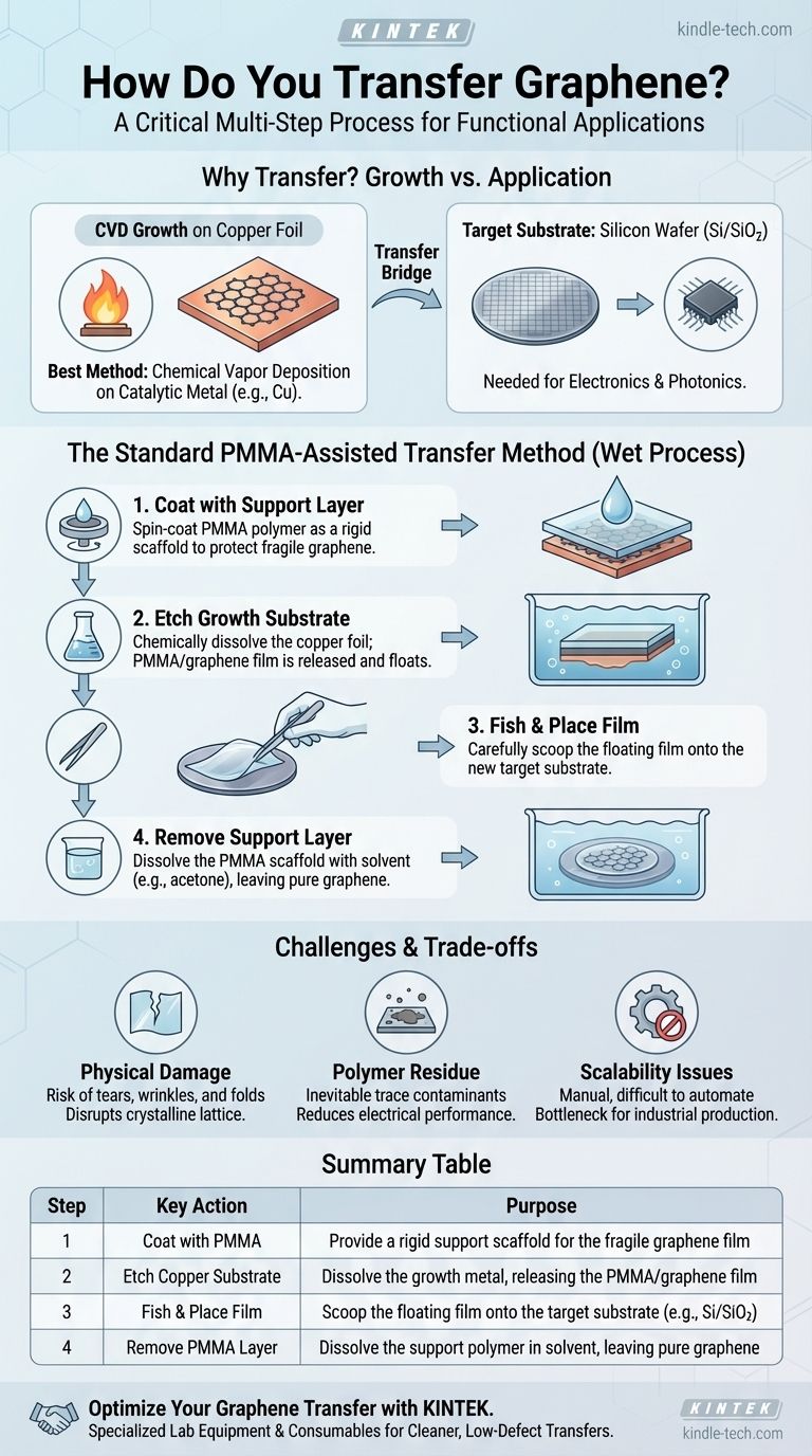
The best method for creating large, high-quality sheets of graphene is Chemical Vapor Deposition (CVD). This process grows graphene on a catalytic metal foil, most commonly copper.
While copper is an excellent substrate for growth, it is not the substrate needed for most electronic or photonic applications. To build a transistor, for example, the graphene must be placed on an insulating substrate like a silicon wafer with a silicon dioxide layer (Si/SiO₂).
The Role of the Growth Substrate
During CVD, hydrocarbon gases decompose at high temperatures, and carbon atoms arrange themselves into the hexagonal lattice of graphene on the surface of the metal catalyst. The result is a continuous graphene film covering the foil. The transfer process is the only way to isolate that film and place it onto a technologically relevant material.
The Standard PMMA-Assisted Transfer Method
This wet-chemical process is the workhorse of graphene research labs worldwide. It can be broken down into four essential steps.
Step 1: Coating with a Support Layer
First, a thin layer of a support polymer, almost always PMMA, is spin-coated on top of the graphene that is sitting on its copper growth foil. This PMMA layer acts like a rigid "handle" or scaffold that protects the fragile graphene during subsequent steps.
Step 2: Etching the Growth Substrate
The PMMA/graphene/copper stack is then placed into a chemical bath, or etchant, that selectively dissolves the copper foil without harming the graphene or PMMA. As the copper is etched away, the transparent PMMA/graphene film is released and left floating on the surface of the liquid.
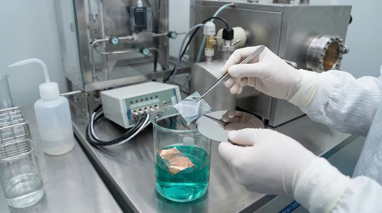
Step 3: "Fishing" and Placing the Film
The floating film is carefully "fished" out of the etchant, typically by dipping the target substrate (e.g., a silicon wafer) into the bath and scooping the film up. The film adheres to the new substrate, and it is then carefully dried.
Step 4: Removing the Support Layer
Finally, the entire sample is bathed in a solvent, such as acetone, that dissolves the PMMA support layer. This final rinse leaves only the pure, single-layer graphene sheet on the target substrate, ready for device fabrication.
Understanding the Trade-offs and Challenges
While standardized, the PMMA wet transfer is not a perfect process. Understanding its limitations is critical for interpreting results and troubleshooting issues.
Risk of Physical Damage
The process is mechanically intensive. Even with the PMMA support, the film can be subject to tears, wrinkles, and folds. These structural defects disrupt the perfect crystalline lattice of graphene and can severely degrade its electrical and mechanical properties.
Inevitable Polymer Residue
Removing 100% of the PMMA support layer is practically impossible. Trace amounts of polymer residue inevitably remain on the graphene surface. This residue acts as a contaminant, scattering charge carriers and reducing the material's performance in electronic devices.
Challenges in Scalability
The standard wet transfer method is largely manual and difficult to automate. This presents a significant bottleneck for the industrial-scale production of graphene-based devices, which would require processing thousands of large-area wafers with high yield and uniformity.
Making the Right Choice for Your Goal
Your application's sensitivity to defects and contamination will determine how you approach the transfer process.
- If your primary focus is lab-scale research and prototyping: The standard PMMA wet transfer method is the established industry practice and is perfectly suitable for creating functional devices.
- If your primary focus is high-performance electronics: Pay meticulous attention to the cleaning and annealing steps after the transfer to minimize polymer residue, as this is a primary factor limiting device performance.
- If your primary focus is industrial-scale production: Investigate emerging automated or "roll-to-roll" transfer techniques that promise higher throughput and better uniformity than manual wet transfers.
Mastering the transfer process is the critical link between synthesizing high-quality graphene and realizing its potential in functional devices.
Summary Table:
| Step | Key Action | Purpose |
|---|---|---|
| 1 | Coat with PMMA | Provide a rigid support scaffold for the fragile graphene film |
| 2 | Etch Copper Substrate | Dissolve the growth metal, releasing the PMMA/graphene film |
| 3 | Fish & Place Film | Scoop the floating film onto the target substrate (e.g., Si/SiO₂) |
| 4 | Remove PMMA Layer | Dissolve the support polymer in solvent, leaving pure graphene |
Need to optimize your graphene transfer process for high-performance devices? KINTEK specializes in providing the precise lab equipment and consumables essential for every step, from spin coaters for uniform PMMA application to chemical baths for controlled etching. Our expertise supports researchers in achieving cleaner transfers with minimal defects and residue. Contact our experts today to discuss how our solutions can enhance your graphene research and development.
Visual Guide
Related Products
- High Purity Pure Graphite Crucible for Evaporation
- High Purity Pure Graphite Crucible for Electron Beam Evaporation
- Chemical Vapor Deposition CVD Equipment System Chamber Slide PECVD Tube Furnace with Liquid Gasifier PECVD Machine
People Also Ask
- Why must high-purity graphite crucibles be treated in a vacuum oven and pre-baked? Ensure Pure Molten Salt Experiments
- Why is a high-purity graphite crucible required for FLiNaK molten salts? Ensure Purity & Data Integrity
- Why are high-purity graphite crucibles used for magnesium distillation? Ensure 3N8 Purity & Thermal Stability
- Why is a high-purity graphite crucible ideal for nitrogen-doped graphene at 1500 °C? Maximize Purity and Stability
- What dual roles do high-purity graphite crucibles play? Expert Insights into Fluoride Salt Testing


