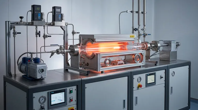
At its core, a Chemical Vapor Deposition (CVD) reactor works by introducing specific gases, called precursors, into a heated, controlled chamber containing the object to be coated (the substrate). These gases undergo a chemical reaction or decomposition directly on the hot substrate surface, depositing a solid, high-performance thin film layer by layer. The entire process is meticulously managed to build materials with precise thickness, purity, and structure.
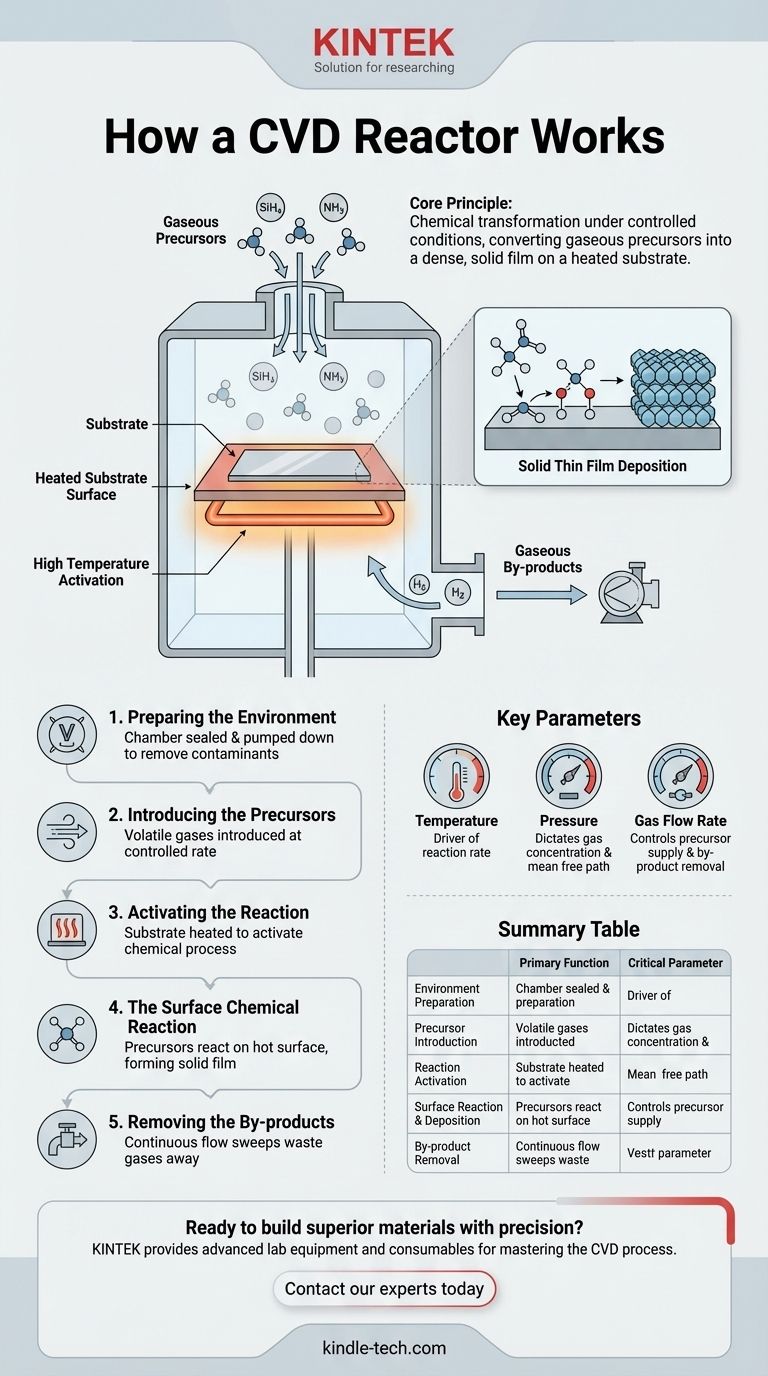
The fundamental principle of a CVD reactor is chemical transformation under controlled conditions. It is not simply "spraying" a material; it is a precise, surface-level chemical reaction that converts gaseous precursors into a dense, solid film on a heated substrate.
The Anatomy of the CVD Process
A CVD reactor is the environment where this transformation from gas to solid occurs. The process can be broken down into a sequence of critical steps, each playing a vital role in the final quality of the coating.
Step 1: Preparing the Environment
Before deposition begins, the substrate is placed inside the reaction chamber. The chamber is typically sealed and pumped down to a vacuum.
This initial vacuum removes air and other potential contaminants, which could otherwise interfere with the chemical reaction and compromise the purity of the final film.
Step 2: Introducing the Precursors
Once the chamber is prepared, one or more volatile precursor gases are introduced at a controlled flow rate. "Volatile" simply means they exist in a gaseous state at relatively low temperatures.
These gases are the building blocks of the final film. For example, to deposit a silicon nitride film, gases like silane (SiH₄) and ammonia (NH₃) might be used.
Step 3: Activating the Reaction with Heat
The substrate itself is heated to a specific, high reaction temperature. This is the most critical step for activating the process.
When the cooler precursor gases come into contact with the hot substrate, they gain the energy needed to react or break down. This localizes the chemical reaction directly onto the surface where the film is desired.
Step 4: The Surface Chemical Reaction
On the hot surface, the precursor molecules undergo chemical processes like decomposition or reaction with other precursors. This reaction forms the desired solid material.
This solid material chemisorbs—or forms a chemical bond—with the substrate surface. This process repeats, building up a dense, solid layer over time, covering all exposed areas.
Step 5: Removing the By-products
The chemical reactions that form the solid film almost always create unwanted gaseous by-products. For instance, the reaction to form silicon (Si) from silane (SiH₄) releases hydrogen gas (H₂).
A continuous gas flow through the chamber is maintained to sweep these by-products out of the reactor. This prevents them from interfering with the deposition process or contaminating the film.
Key Parameters That Define the Outcome
The quality, thickness, and properties of the deposited film are not accidental. They are the direct result of carefully controlling several key variables within the reactor.
The Role of Temperature
Temperature is the primary driver of the reaction rate. Higher temperatures generally lead to faster deposition but can also affect the crystalline structure of the film. An incorrect temperature can result in poor adhesion or a flawed film.
The Importance of Pressure
Pressure inside the chamber dictates the concentration of precursor gases and the distance molecules travel before colliding. Low-pressure (vacuum) systems are common because they enhance film purity and uniformity by increasing the mean free path of gas molecules, ensuring they reach the substrate without reacting prematurely in the gas phase.
The Function of Gas Flow Rate
The flow rate controls the supply of fresh precursor gas to the substrate and the rate at which by-products are removed. A flow rate that is too low can starve the reaction, while one that is too high can waste precursor material and disrupt uniform deposition.
Understanding the Trade-offs and Limitations
While powerful, the CVD process has inherent challenges that are important to understand when selecting a coating technology.
Line-of-Sight Dependency
CVD relies on gas being able to physically reach the substrate surface to react. This can make it difficult to uniformly coat the inside of very long, narrow tubes or complex internal geometries where gas flow is restricted.
High-Temperature Requirements
The high temperatures required to activate the chemical reactions can damage heat-sensitive substrates, such as many polymers or pre-assembled electronic components. This limits the types of materials that can be coated with standard CVD methods.
Precursor Chemistry and Safety
The gases used as precursors are often highly reactive, toxic, flammable, or corrosive. Operating a CVD reactor therefore requires significant safety infrastructure and specialized handling procedures.
Applying This to Your Material Goal
Understanding how a CVD reactor works allows you to tailor the process to a specific objective.
- If your primary focus is a perfectly uniform, crystalline film (e.g., for semiconductors): Your most critical variables are precise temperature control and a stable, low-pressure environment to ensure orderly, layer-by-layer growth.
- If your primary focus is a hard, protective coating on a complex part: You must ensure the gas flow dynamics are engineered to allow precursors to reach all critical surfaces, otherwise the coating will lack uniformity.
- If your primary focus is maximizing deposition speed: You will need to balance higher precursor concentrations and temperatures against the risk of reduced film quality and the formation of unwanted powder from gas-phase reactions.
Ultimately, mastering the CVD process is about mastering the interplay between chemistry, heat, and gas dynamics to build materials from the ground up.
Summary Table:
| Key CVD Reactor Step | Primary Function | Critical Parameter |
|---|---|---|
| Environment Preparation | Remove contaminants for high-purity film | Vacuum level |
| Precursor Introduction | Supply building-block gases to the chamber | Gas flow rate |
| Reaction Activation | Provide energy for surface chemical reaction | Substrate temperature |
| Surface Reaction & Deposition | Form solid film layer-by-layer on the substrate | Precursor chemistry |
| By-product Removal | Sweep away waste gases to maintain film quality | Chamber pressure & flow dynamics |
Ready to build superior materials with precision?
At KINTEK, we specialize in providing the advanced lab equipment and consumables you need to master the CVD process. Whether you are developing semiconductor films, protective coatings, or novel materials, our expertise and reliable solutions ensure your reactor operates at peak performance.
Let's discuss your specific application and material goals. Contact our experts today to find the perfect CVD solution for your laboratory.
Visual Guide
Related Products
- Cylindrical Resonator MPCVD Machine System Reactor for Microwave Plasma Chemical Vapor Deposition and Lab Diamond Growth
- Customer Made Versatile CVD Tube Furnace Chemical Vapor Deposition Chamber System Equipment
- Microwave Plasma Chemical Vapor Deposition MPCVD Machine System Reactor for Lab and Diamond Growth
- 915MHz MPCVD Diamond Machine Microwave Plasma Chemical Vapor Deposition System Reactor
- Split Chamber CVD Tube Furnace with Vacuum Station Chemical Vapor Deposition System Equipment Machine
People Also Ask
- Why is argon-rich gas phase chemistry used for UNCD growth? Unlock Precision Nano-Diamond Synthesis
- What are the advantages of a Microwave Plasma CVD reactor for MCD/NCD coatings? Precision Multilayer Diamond Engineering
- How is a diamond formed from CVD? The Science of Growing Diamonds Atom by Atom
- How does a microwave plasma reactor facilitate the synthesis of diamond? Master MPCVD with Precision Technology
- What pressure is needed for chemical vapor deposition of diamonds? Master the Low-Pressure 'Sweet Spot'