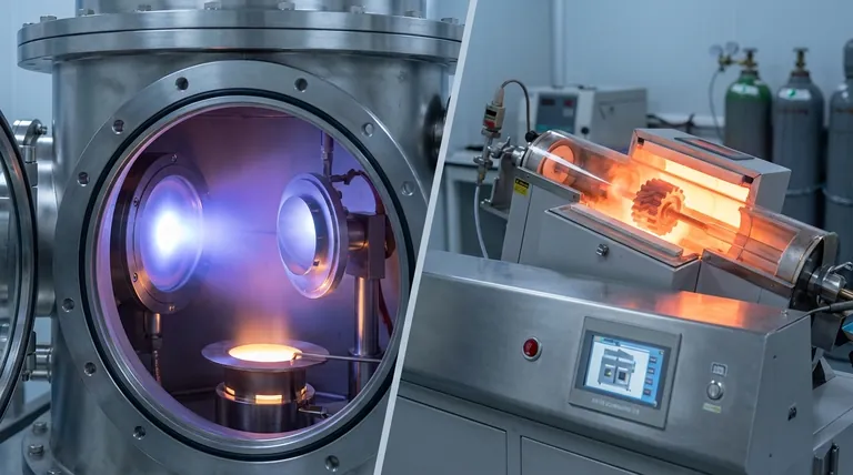
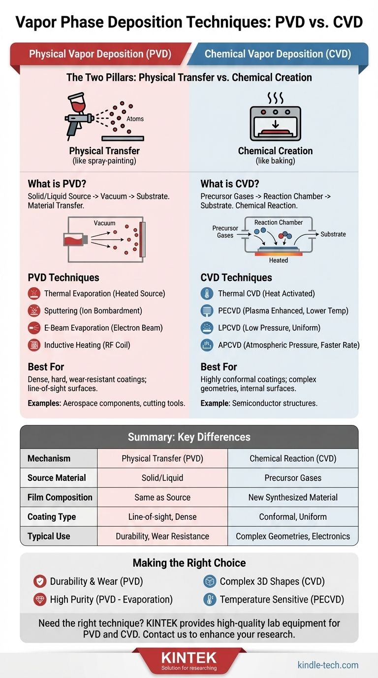
At the highest level, there are two fundamental types of vapor phase deposition: Physical Vapor Deposition (PVD) and Chemical Vapor Deposition (CVD). PVD involves the physical transfer of a material from a source to a substrate, typically from a solid or liquid state. In contrast, CVD uses chemical reactions between precursor gases to synthesize a new solid material directly onto the substrate's surface.
The critical distinction is not the number of techniques, but the core mechanism. PVD is a process of physical transfer, like spray-painting with atoms. CVD is a process of chemical creation, like baking a new solid layer onto a surface from gas-phase ingredients.
The Two Pillars: PVD and CVD
The choice between PVD and CVD is the first and most important decision, as it defines the entire deposition process, from the source materials used to the properties of the final film.
What is Physical Vapor Deposition (PVD)?
PVD techniques use a solid or liquid source material. This material is vaporized in a vacuum environment and then transported to the substrate, where it condenses to form the desired thin film.
The key characteristic of PVD is that the deposited material is the same as the source material, just transferred from one place to another.
What is Chemical Vapor Deposition (CVD)?
CVD techniques begin with one or more volatile precursor gases introduced into a reaction chamber. These gases decompose or react near or on a heated substrate to form a solid film.
The deposited material in CVD is a new substance synthesized by the chemical reaction, not a direct transfer of a source material.
Exploring Physical Vapor Deposition (PVD) Techniques
PVD methods are primarily categorized by how the source material is vaporized. These are line-of-sight processes, meaning the source must have a clear path to the substrate.
Thermal Evaporation
This is a foundational PVD method. A source material is heated by a resistive element in a high vacuum until it evaporates or sublimes. The vapor then travels and condenses on the cooler substrate.
Sputtering
In sputtering, a target made of the source material is bombarded with high-energy ions (usually an inert gas plasma like Argon). This bombardment physically ejects atoms from the target, which then deposit onto the substrate.
Electron-Beam (E-Beam) Evaporation
This is a more precise form of thermal evaporation. A high-energy, focused electron beam heats the source material, causing it to evaporate. This allows for the deposition of materials with very high melting points.
Inductive Heating
In this method, Radio Frequency (RF) power is run through a metal coil. This coil is typically wound around a crucible containing the source material, inducing eddy currents that heat the crucible and evaporate the material inside.
Exploring Chemical Vapor Deposition (CVD) Techniques
CVD methods are categorized by the conditions used to initiate and sustain the chemical reaction, such as temperature, pressure, or the use of plasma.
Activation by Heat (Thermally Activated CVD)
This is the most common form of CVD. The substrate is heated to a high temperature, providing the thermal energy needed to break the chemical bonds in the precursor gases and drive the deposition reaction.
Activation by Plasma (Plasma-Enhanced CVD)
Plasma-Enhanced CVD (PECVD) uses an electric field to generate a plasma (a highly reactive ionized gas). The plasma provides the energy to break apart the precursor gas molecules, allowing deposition to occur at much lower temperatures than in thermally activated CVD.
The Role of Pressure (LPCVD vs. APCVD)
CVD processes are also defined by their operating pressure. In Low-Pressure CVD (LPCVD), the reaction is limited by the rate of the surface chemical reaction itself, leading to very uniform and conformal coatings.
In Atmospheric-Pressure CVD (APCVD), the reaction is limited by how fast the precursor gases can be transported to the surface, known as the mass transfer rate.
Understanding the Trade-offs: PVD vs. CVD
Choosing the right method depends entirely on the desired properties of the final film and the geometry of the part being coated.
When to Choose PVD
PVD excels at creating dense, hard, and wear-resistant coatings. Because it is a line-of-sight physical process, it is ideal for coating surfaces that directly face the source material.
Applications like applying temperature-resistant coatings on aerospace components or hard, corrosion-resistant films on cutting tools are classic use cases for PVD.
When to Choose CVD
CVD's greatest strength is its ability to produce highly conformal coatings. Because the precursor gases can flow around and into complex geometries, CVD can uniformly coat intricate shapes, trenches, and internal surfaces where PVD cannot reach.
This makes it indispensable in the semiconductor industry for depositing uniform layers inside complex microelectronic structures.
Making the Right Choice for Your Goal
Ultimately, the technique you choose must align with your primary objective for the thin film.
- If your primary focus is durability and wear resistance on a direct-facing surface: PVD techniques like sputtering or e-beam evaporation are the industry standard.
- If your primary focus is creating a uniform, conformal coating over a complex 3D shape: CVD is the superior choice due to the nature of its gas-phase chemical reactions.
- If your primary focus is depositing a high-purity metallic or optical film: PVD methods, particularly evaporation, offer excellent control over material purity and composition.
- If your primary focus is depositing a film on a temperature-sensitive substrate: Plasma-Enhanced CVD (PECVD) allows for high-quality film growth at significantly lower temperatures.
Understanding this fundamental split between physical transfer (PVD) and chemical creation (CVD) is the key to navigating the options and selecting the right process for your specific application.
Summary Table:
| Category | Key Technique | Primary Mechanism | Best For |
|---|---|---|---|
| Physical Vapor Deposition (PVD) | Thermal Evaporation, Sputtering, E-Beam | Physical transfer of source material | Dense, hard coatings; line-of-sight surfaces |
| Chemical Vapor Deposition (CVD) | Thermal CVD, PECVD, LPCVD | Chemical reaction of precursor gases | Conformal coatings; complex 3D geometries |
Need to select the right vapor phase deposition technique for your specific application? KINTEK specializes in providing high-quality lab equipment and consumables for all your deposition needs. Whether you require the durability of PVD systems or the conformal coating capabilities of CVD, our experts can help you choose the perfect solution to enhance your research and production outcomes. Contact our team today to discuss your project requirements and discover how KINTEK can support your laboratory's success!
Visual Guide
Related Products
- RF PECVD System Radio Frequency Plasma-Enhanced Chemical Vapor Deposition RF PECVD
- Chemical Vapor Deposition CVD Equipment System Chamber Slide PECVD Tube Furnace with Liquid Gasifier PECVD Machine
- 915MHz MPCVD Diamond Machine Microwave Plasma Chemical Vapor Deposition System Reactor
- Microwave Plasma Chemical Vapor Deposition MPCVD Machine System Reactor for Lab and Diamond Growth
- Inclined Rotary Plasma Enhanced Chemical Vapor Deposition PECVD Equipment Tube Furnace Machine
People Also Ask
- What is an example of PECVD? RF-PECVD for High-Quality Thin Film Deposition
- What is plasma chemical vapor deposition? A Low-Temperature Thin Film Coating Solution
- What is the role of RF-PECVD in VFG preparation? Mastering Vertical Growth and Surface Functionality
- Why is a Matching Network Indispensable in RF-PECVD for Siloxane Films? Ensure Stable Plasma and Uniform Deposition
- How does plasma enhance CVD? Unlock Low-Temperature, High-Quality Film Deposition


