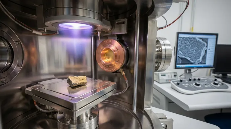
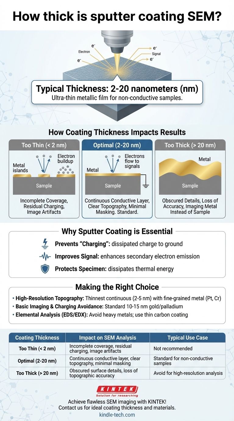
In scanning electron microscopy (SEM), the typical thickness of a sputter coating is between 2 and 20 nanometers (nm). This ultra-thin metallic film is applied to non-conductive or poorly conductive samples to prevent electrical charging and improve image quality, providing a stable and clear view of the specimen's surface under the electron beam.
The core principle of sputter coating is to apply the thinnest possible conductive layer that effectively dissipates charge without obscuring the sample's true surface topography. The goal is intervention, not alteration.
Why Sputter Coating is Essential for Non-Conductive Samples
Sputter coating solves a fundamental physics problem that arises when an electron beam interacts with an insulating material. Without it, obtaining a clear, stable image is often impossible.
The Problem of "Charging"
When the high-energy electron beam of an SEM strikes a non-conductive sample, the electrons have no path to ground. They accumulate on the surface.
This buildup of negative charge, known as specimen charging, deflects the incoming electron beam and distorts the emitted signal, resulting in bright patches, streaks, and a loss of image detail.
Improving Signal for Better Images
A sputter-coated metallic layer provides an effective conductive path, allowing the excess charge to dissipate to the grounded SEM stage.
Furthermore, heavy metals like gold and platinum are excellent emitters of secondary electrons—the primary signal used for creating topographic images in an SEM. This coating enhances the signal-to-noise ratio, producing sharper and more detailed images.
Protecting the Specimen
The electron beam imparts a significant amount of energy into a very small area, which can cause thermal damage to delicate biological or polymeric samples.
The conductive metal coating helps dissipate this thermal energy away from the point of impact, protecting the specimen's fine structure from being altered or destroyed by the beam.
How Coating Thickness Impacts Your Results
The 2-20 nm range is not arbitrary. The specific thickness is a critical parameter that directly influences the quality and accuracy of your analysis.
The "Too Thin" Problem
A coating that is too thin (typically below 2 nm) may not form a continuous, uniform film. Instead, it can form disconnected "islands" of metal.
This incomplete coverage fails to provide a consistent path to ground, leading to residual charging and image artifacts, defeating the purpose of the coating process.
The "Too Thick" Problem
As the coating thickness increases, it begins to obscure the sample's native surface features. A layer that is too thick will mask fine details like pores, grain boundaries, or nanoparticles.
At this point, you are no longer imaging the specimen itself, but rather a metal casting of it. This significantly reduces the accuracy of topographical analysis.
Finding the Optimal Balance
The ideal coating is the thinnest possible layer that remains fully continuous and conductive. This balance ensures charge dissipation while minimizing any masking of the sample's true surface, which is why the 2-20 nm range is the industry standard.
Understanding the Trade-offs of Sputter Coating
While essential, sputter coating is an interventive technique. Acknowledging its drawbacks is crucial for accurate data interpretation.
Obscured Surface Features
Any coating, no matter how thin, adds a layer on top of the true surface. For ultra-high-resolution imaging of nanoscale features, even a few nanometers of gold can alter the perceived topography.
Loss of Compositional Data
Sputter coating fundamentally compromises elemental analysis, such as Energy-Dispersive X-ray Spectroscopy (EDS/EDX).
The coating material (e.g., gold, platinum) will produce a strong signal in the EDS spectrum, which can overlap with and mask the signals from elements within the actual sample. This is often referred to as a loss of atomic number contrast.
The Need for Careful Calibration
Achieving a specific thickness is not an automatic process. It requires careful calibration and optimization of parameters like coating time, electrical current, and chamber pressure for each specific material and sample type.
Making the Right Choice for Your Analysis
Your analytical goal should dictate your coating strategy. The ideal approach balances the need for conductivity with the need for data fidelity.
- If your primary focus is high-resolution surface topography: Aim for the thinnest possible continuous coating (e.g., 2-5 nm) using a fine-grained metal like platinum or chromium to minimize artifacts.
- If your primary focus is basic imaging and avoiding charging: A standard 10-15 nm gold or gold/palladium coating is a reliable and cost-effective choice that works well for a wide range of samples.
- If your primary focus is elemental analysis (EDS/EDX): Avoid heavy metal sputter coating entirely. Instead, use a sputter coater to apply a thin layer of carbon, which interferes far less with elemental signals.
Ultimately, successful SEM preparation is about applying the minimum intervention necessary to acquire the data you need.
Summary Table:
| Coating Thickness | Impact on SEM Analysis | Typical Use Case |
|---|---|---|
| Too Thin (< 2 nm) | Incomplete coverage, residual charging, image artifacts | Not recommended; fails to prevent charging |
| Optimal (2-20 nm) | Continuous conductive layer, clear topography, minimal feature masking | Standard for non-conductive samples (e.g., 10-15 nm gold for general imaging) |
| Too Thick (> 20 nm) | Obscured surface details, loss of topographic accuracy | Avoid for high-resolution analysis; risks imaging the metal layer instead of the sample |
Achieve flawless SEM imaging with precision sputter coating from KINTEK!
Struggling with charging artifacts or unclear results? Our expert team will help you select the ideal coating thickness and material (like gold, platinum, or carbon) tailored to your sample and analysis goals. We specialize in lab equipment and consumables to meet all your laboratory needs.
Contact us today for a consultation and elevate your SEM sample preparation!
Visual Guide
Related Products
- Custom CVD Diamond Coating for Lab Applications
- HFCVD Machine System Equipment for Drawing Die Nano-Diamond Coating
- Chemical Vapor Deposition CVD Equipment System Chamber Slide PECVD Tube Furnace with Liquid Gasifier PECVD Machine
- Multifunctional Electrolytic Electrochemical Cell Water Bath Single Layer Double Layer
- Professional Cutting Tools for Carbon Paper Cloth Diaphragm Copper Aluminum Foil and More
People Also Ask
- What is CVD coating? Transform Your Material's Surface for Maximum Performance
- What is the use of CVD coating? Enhance Durability and Functionality for Your Components
- What are the different CVD coating? A Guide to Thermal CVD, PECVD, and Specialized Methods
- What is CVD coated? A Guide to Superior Wear Resistance for Complex Parts
- What are the types of CVD coating? A Guide to Choosing the Right Process


