Yes, absolutely. Deposition technology is not just a single advancement, but a foundational family of techniques that represents one of the most critical, yet often invisible, pillars of our modern world. Without the ability to precisely deposit ultra-thin layers of materials—often just a few atoms thick—the computer chips, solar panels, and advanced tools we rely on simply would not exist.
Deposition technology's true significance lies in its core function: it gives us control over matter at the atomic scale. It is the manufacturing process that allows us to build the fundamental structures of virtually all high-performance electronic and material-based products.
What is Deposition? A Foundation for the Modern World
At its heart, deposition is the process of applying a thin film of material onto a surface, known as a substrate.
Think of it like spray painting, but on an unimaginably small scale. Instead of paint, you are depositing individual atoms or molecules. Instead of a canvas, you might have a silicon wafer or a medical implant.
The Core Principle: Building From the Bottom Up
The goal of deposition is to create a new layer on a surface that has specific, desirable properties. This new layer, or thin film, can make the object stronger, more conductive, resistant to corrosion, or give it unique optical or electrical functions.
This "bottom-up" manufacturing is the opposite of traditional "subtractive" manufacturing, where you start with a block of material and cut away what you don't need.
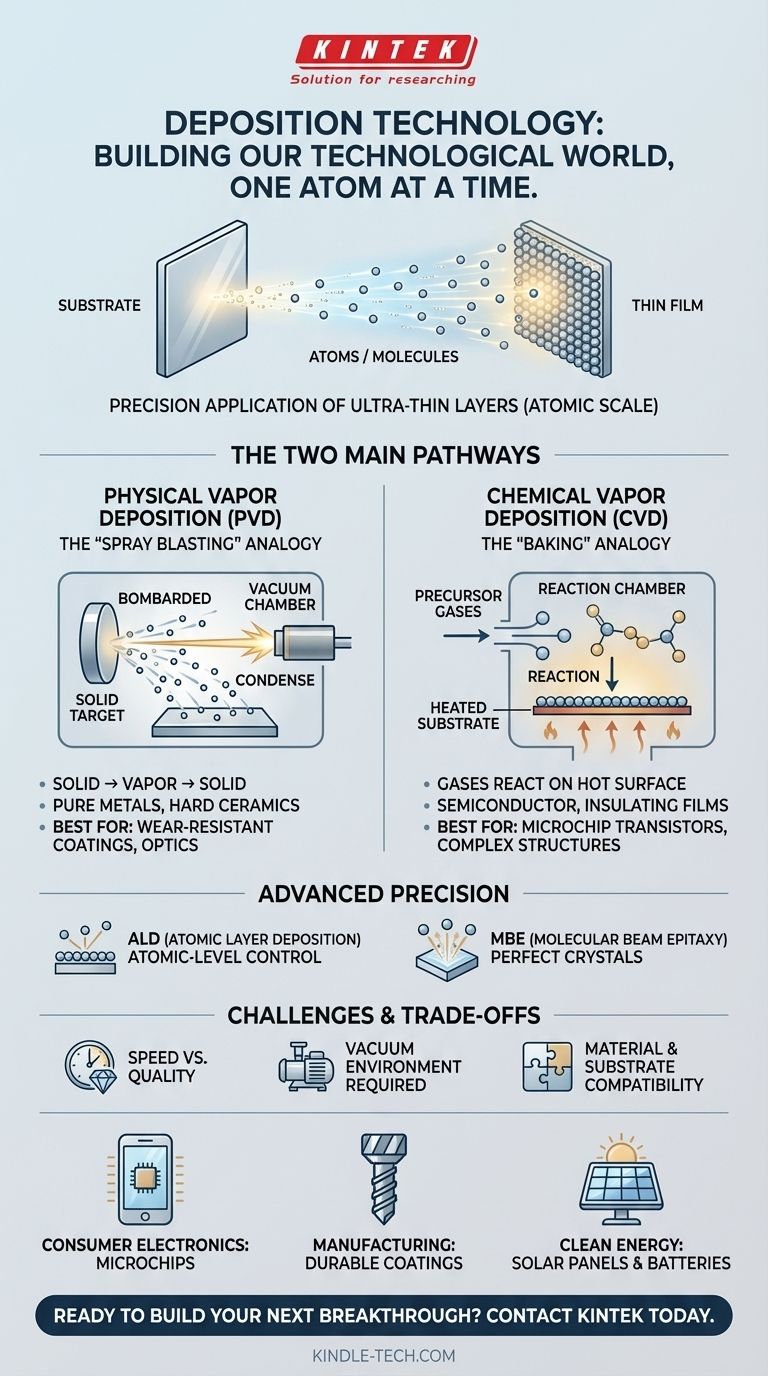
From Vapor to Solid: The Two Main Pathways
Nearly all deposition techniques fall into one of two major categories, defined by how they transport the material to the surface.
- Physical Vapor Deposition (PVD): The material starts as a solid, is turned into a vapor through physical means (like heating or bombardment with ions), travels through a vacuum, and then condenses back into a solid on the substrate.
- Chemical Vapor Deposition (CVD): Precursor gases are introduced into a reaction chamber. These gases react or decompose on the hot substrate surface, leaving behind the desired solid material as a thin film.
The Two Pillars of Deposition Technology
Understanding the difference between PVD and CVD is key to appreciating the breadth of what deposition can accomplish. Each is a world unto itself, with specific techniques suited for different applications.
Physical Vapor Deposition (PVD): The "Spray Blasting" Analogy
PVD processes are like an atomic-scale sandblaster operating in reverse. A solid "target" of the material you want to deposit is bombarded with energy, which ejects atoms that then fly across a vacuum chamber and coat the substrate.
This method is excellent for depositing very pure metals and hard, durable ceramic compounds. It's used to create the wear-resistant coatings on drill bits, the low-friction surfaces on engine parts, and the reflective layers on glass and optics.
Chemical Vapor Deposition (CVD): The "Baking" Analogy
CVD is more like baking a cake. You mix specific ingredients (precursor gases) and use heat to trigger a chemical reaction on the surface of the substrate. This reaction "bakes" a solid layer onto the surface.
CVD is the absolute workhorse of the semiconductor industry. It is essential for creating the incredibly complex, layered structures of transistors and interconnects on a microchip. The precise control over chemical reactions allows for the creation of high-purity insulating, conducting, and semiconducting films.
Beyond the Basics: Precision Perfected
More advanced techniques offer even greater control. Atomic Layer Deposition (ALD), a subtype of CVD, builds a material literally one atomic layer at a time, offering unparalleled precision for the most advanced microchips. Molecular Beam Epitaxy (MBE) allows for the creation of perfect, single-crystal films used in high-frequency electronics and lasers.
Understanding the Trade-offs and Challenges
While deposition technology is powerful, it is not without significant engineering challenges. These trade-offs define its application and cost.
The Constant Battle: Speed vs. Quality
Generally, the faster you deposit a film, the lower its quality (less uniform, more defects). Highly precise processes like ALD produce near-perfect films but are extremely slow, making them expensive and suitable only for the most critical, thinnest layers.
The Challenge of a Vacuum
Most PVD and some CVD processes require a high-vacuum environment to prevent contamination and allow atoms to travel freely. Creating and maintaining this vacuum requires complex, expensive equipment and adds significantly to the manufacturing cost and complexity.
Material and Substrate Limitations
Not every material can be easily deposited, and not every film will stick well to every substrate. A great deal of research goes into finding the right process parameters, precursor chemicals, and surface preparation techniques to ensure a strong, functional bond between the film and the surface it's on.
Making the Right Choice for Your Goal
The "best" deposition method is entirely dependent on the desired outcome. Its impact is best understood by looking at its purpose in different fields.
- If your primary focus is consumer electronics: You should know that every single microchip in your phone or computer is built using a sequence of dozens, if not hundreds, of CVD and PVD steps to create its transistors and wiring.
- If your primary focus is manufacturing and engineering: You can look to PVD coatings as the technology that dramatically extends the life of cutting tools, reduces friction in engines, and protects components from corrosion.
- If your primary focus is clean energy: You should recognize that both the light-absorbing layers in many solar panels and the critical protective films in modern batteries are created using various deposition techniques.
Deposition technology is the unsung art of building our technological world, one atomic layer at a time.
Summary Table:
| Aspect | PVD (Physical Vapor Deposition) | CVD (Chemical Vapor Deposition) |
|---|---|---|
| Process | Solid target vaporized, condenses on substrate | Gases react on hot surface to form solid film |
| Best For | Pure metals, hard ceramic coatings | High-purity semiconductor, insulating films |
| Key Use | Wear-resistant coatings, optics | Microchip transistors, complex layered structures |
| Precision | High | Extremely high (e.g., ALD: atomic layer control) |
Ready to Build Your Next Breakthrough with Precision Deposition?
At KINTEK, we specialize in providing the advanced lab equipment and consumables needed to harness the power of deposition technology. Whether you're developing next-generation microchips, durable industrial coatings, or efficient solar panels, our solutions are designed to meet the rigorous demands of modern research and manufacturing.
Let KINTEK empower your lab to:
- Achieve atomic-scale precision with reliable PVD and CVD systems.
- Enhance product performance with high-quality thin films.
- Accelerate your R&D with industry-leading equipment and support.
Don't let technical challenges slow your innovation. Contact our experts today to discuss how our specialized lab equipment can drive your projects forward!
Visual Guide
Related Products
- Chemical Vapor Deposition CVD Equipment System Chamber Slide PECVD Tube Furnace with Liquid Gasifier PECVD Machine
- RF PECVD System Radio Frequency Plasma-Enhanced Chemical Vapor Deposition RF PECVD
- Microwave Plasma Chemical Vapor Deposition MPCVD Machine System Reactor for Lab and Diamond Growth
- Customer Made Versatile CVD Tube Furnace Chemical Vapor Deposition Chamber System Equipment
- Split Chamber CVD Tube Furnace with Vacuum Station Chemical Vapor Deposition System Equipment Machine
People Also Ask
- How are carbon nanotubes grown? Master Scalable Production with Chemical Vapor Deposition
- What happens during deposition chemistry? Building Thin Films from Gaseous Precursors
- What types of substrates are used in CVD to facilitate graphene films? Optimize Graphene Growth with the Right Catalyst
- What is the chemical vapor deposition growth process? Build Superior Thin Films from the Atom Up
- How expensive is chemical vapor deposition? Understanding the True Cost of High-Performance Coating


