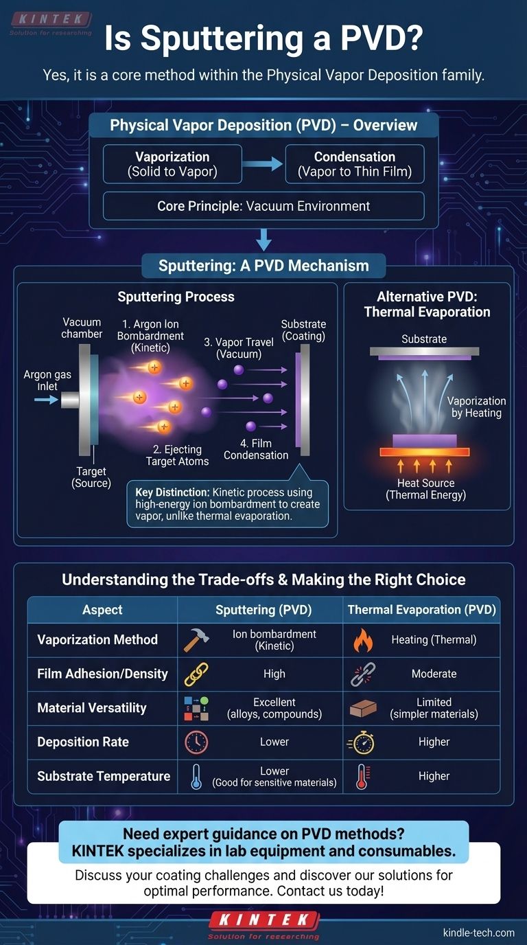
Yes, sputtering is a core method of Physical Vapor Deposition (PVD). Sputtering is not a separate category but rather a specific mechanism used within the broader P_VD_ family of techniques. It is a process that physically ejects atoms from a solid source material, called a target, so they can travel through a vacuum and deposit onto a substrate as a thin film.
The critical distinction to understand is that Physical Vapor Deposition (PVD) is the overarching category of coating processes performed in a vacuum. Sputtering is a specific technique within that category that uses high-energy ion bombardment to create the vapor, distinguishing it from other PVD methods like thermal evaporation.
What Defines a PVD Process?
To understand where sputtering fits, we must first define the parent category. All PVD processes share two fundamental characteristics.
The Core Principle: A Vacuum Environment
All PVD methods take place in a vacuum chamber. This controlled environment is critical because it removes atmospheric gases that could otherwise react with the coating material or interfere with its path to the substrate.
The Two-Step Process
At its heart, PVD is a simple sequence:
- Vaporization: A solid source material is converted into a vapor.
- Condensation: This vapor travels and condenses on a substrate, forming a solid thin film.
The key difference between PVD methods lies in how they achieve the vaporization step.
How Sputtering Works as a PVD Process
Sputtering accomplishes the vaporization step through a purely physical, kinetic process, almost like an atomic-scale sandblasting operation.
The Mechanism: Ion Bombardment
The process begins by introducing an inert gas, typically argon, into the vacuum chamber. An electric field is applied, which ignites the gas and creates a plasma—a cloud of energized ions.
These positively charged argon ions are accelerated with high energy toward the negatively charged source material, or target.
Creating the Vapor
When these high-energy ions collide with the target, they transfer their momentum, physically knocking out or "sputtering" atoms from the target's surface. These ejected atoms travel through the vacuum chamber.
This cloud of ejected target material is the "vapor" in Physical Vapor Deposition.
Condensing into a Film
The sputtered atoms travel in a straight line until they strike the substrate, where they condense and build up layer-by-layer to form a dense, uniform, and highly adherent thin film.
Understanding the Trade-offs
Sputtering is one of the most versatile and widely used PVD techniques, but it's important to understand its advantages and limitations compared to other methods like thermal evaporation.
The Primary Advantage: Material Versatility
Sputtering's key strength is its ability to deposit a vast range of materials, including complex alloys, compounds, and high-temperature refractory metals. Because the atoms are physically ejected rather than boiled, the composition of the deposited film can be kept very close to that of the source target.
The Primary Alternative: Thermal Evaporation
The other major PVD method is thermal evaporation. Instead of using kinetic bombardment, this technique simply heats the source material in the vacuum until it evaporates (or sublimates), creating a vapor that then condenses on the substrate.
Key Considerations
Sputtering generally produces films with higher density and better adhesion than evaporation due to the higher kinetic energy of the deposited atoms. However, deposition rates for sputtering can be lower than for some evaporation processes.
Making the Right PVD Choice
Choosing between sputtering and other PVD methods depends entirely on the material you are depositing and the desired properties of the final film.
- If your primary focus is depositing complex alloys or compounds: Sputtering provides superior control over the film's chemical composition (stoichiometry).
- If your primary focus is coating heat-sensitive substrates: Sputtering is often a lower-temperature process compared to thermal evaporation, making it ideal for plastics and other sensitive materials.
- If your primary focus is achieving maximum film adhesion and density: The energetic nature of the sputtering process typically results in exceptionally dense and strongly bonded films.
By recognizing sputtering as a powerful and versatile PVD mechanism, you can better select the precise coating technology to meet your project's demands.
Summary Table:
| Aspect | Sputtering (PVD) | Thermal Evaporation (PVD) |
|---|---|---|
| Vaporization Method | Ion bombardment (kinetic energy) | Heating (thermal energy) |
| Film Adhesion/Density | High | Moderate |
| Material Versatility | Excellent (alloys, compounds, refractory metals) | Limited (simpler materials) |
| Typical Deposition Rate | Lower | Higher |
| Substrate Temperature | Lower (good for heat-sensitive materials) | Higher |
Need expert guidance on selecting the right PVD method for your project? KINTEK specializes in lab equipment and consumables, serving laboratory needs. Whether you're depositing complex alloys, working with heat-sensitive substrates, or require high-density films, our sputtering systems and expertise ensure optimal performance. Contact us today to discuss your specific coating challenges and discover how our solutions can enhance your research and production outcomes!
Visual Guide
Related Products
- RF PECVD System Radio Frequency Plasma-Enhanced Chemical Vapor Deposition RF PECVD
- Inclined Rotary Plasma Enhanced Chemical Vapor Deposition PECVD Equipment Tube Furnace Machine
- Inclined Rotary Plasma Enhanced Chemical Vapor Deposition PECVD Equipment Tube Furnace Machine
- Cylindrical Resonator MPCVD Machine System Reactor for Microwave Plasma Chemical Vapor Deposition and Lab Diamond Growth
- HFCVD Machine System Equipment for Drawing Die Nano-Diamond Coating
People Also Ask
- What is plasma activated chemical vapour deposition method? A Low-Temperature Solution for Advanced Coatings
- What is an example of PECVD? RF-PECVD for High-Quality Thin Film Deposition
- What are the benefits of PECVD? Achieve Superior Low-Temperature Thin Film Deposition
- What are the applications of PECVD? Essential for Semiconductors, MEMS, and Solar Cells
- What is the principle of plasma enhanced chemical vapor deposition? Achieve Low-Temperature Thin Film Deposition