At its core, metal deposition is accomplished through two primary families of techniques: Physical Vapor Deposition (PVD), where a solid material is vaporized in a vacuum and condensed onto a surface, and Chemical Deposition, where a chemical reaction on a surface forms the metallic film. Common PVD methods include evaporation and sputtering, while chemical approaches include Chemical Vapor Deposition (CVD), Atomic Layer Deposition (ALD), and plating.
The critical insight is not which deposition method is "best," but which one offers the right balance of film quality, thickness control, cost, and substrate compatibility for your specific application. The choice is always dictated by the desired outcome.
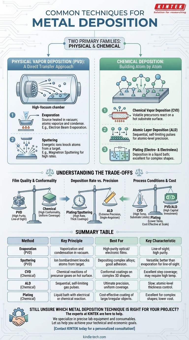
Physical Vapor Deposition (PVD): A Direct Transfer Approach
PVD techniques are fundamentally mechanical at the atomic level. They take place in a high-vacuum chamber, where atoms are physically ejected from a source material and travel in a straight line to deposit onto the target substrate.
The Principle of Evaporation
In evaporation, a source metal is heated in a vacuum until its atoms vaporize. These gaseous atoms travel through the chamber and condense on the cooler substrate, forming a thin film.
Electron beam evaporation is a common, high-purity version of this process. It uses a focused beam of electrons to heat the source material with great precision.
The Principle of Sputtering
Sputtering uses energetic ions, typically from a plasma, to bombard a source material (the "target"). This atomic-scale collision physically knocks off, or "sputters," atoms from the target, which then deposit onto the substrate.
Magnetron sputtering is an advanced form that uses magnetic fields to trap electrons near the target, dramatically increasing the efficiency of the ion bombardment and leading to higher deposition rates.
Chemical Deposition: Building Atom by Atom
Unlike PVD, chemical deposition techniques rely on controlled chemical reactions that occur directly on the substrate's surface. These methods "build" the film from precursor materials rather than transferring it whole.
Chemical Vapor Deposition (CVD)
In CVD, the substrate is placed in a reaction chamber and heated. Volatile precursor gases are introduced, which react or decompose on the hot surface to form the desired solid film.
Atomic Layer Deposition (ALD)
ALD is a specialized subtype of CVD that offers the highest level of precision. It works by introducing precursor gases in sequential, self-limiting pulses, allowing you to build a film one single atomic layer at a time.
Plating (Electro- and Electroless)
Plating is a chemical deposition technique that occurs in a liquid chemical bath. It is highly effective for coating complex shapes.
Electroplating uses an external electrical current to drive the deposition of metal ions from a solution onto the substrate. Electroless plating achieves a similar result through an autocatalytic chemical reaction without any external power.
Understanding the Trade-offs
No single method is universally superior. The optimal choice depends entirely on balancing competing priorities for your project.
Film Quality and Conformality
PVD methods like evaporation and sputtering produce very high-purity films but are "line-of-sight" processes. This makes it difficult to evenly coat complex, three-dimensional shapes.
Chemical methods like ALD and CVD excel at producing highly conformal coatings, meaning they can uniformly cover intricate topographies, trenches, and cavities.
Deposition Rate vs. Precision
Plating and magnetron sputtering can offer very high deposition rates, making them suitable for creating thick coatings cost-effectively.
In contrast, ALD is an extremely slow process. Its value lies in its unparalleled precision and ability to control film thickness down to the single-angstrom level.
Process Conditions and Cost
High-temperature processes like CVD can limit the types of substrates that can be used without damage. Sputtering and plating can often be performed at much lower temperatures.
Vacuum-based PVD and ALD systems represent a significant capital investment, whereas chemical bath deposition or plating can sometimes be implemented at a lower cost, especially at scale.
Selecting the Right Deposition Method
Your primary goal is the most important factor in determining the correct technique.
- If your primary focus is ultimate precision and uniform coverage on complex 3D parts: ALD is the definitive choice for its atomic-level control.
- If your primary focus is high-purity films for optical or electronic applications: PVD methods like e-beam evaporation or sputtering are ideal.
- If your primary focus is cost-effective coating of large or irregular objects: Electroplating or electroless plating often provides the most practical and scalable solution.
- If your primary focus is depositing complex alloys with a specific composition: Sputtering offers excellent control over the final film's stoichiometry.
Ultimately, understanding the fundamental principles of each method empowers you to select the process that best aligns with your technical and economic goals.
Summary Table:
| Method | Key Principle | Best For | Key Characteristic |
|---|---|---|---|
| Evaporation (PVD) | Heating a source material in a vacuum until it vaporizes and condenses on a substrate. | High-purity films for optical/electronic applications. | Line-of-sight deposition; excellent purity. |
| Sputtering (PVD) | Using ion bombardment to knock atoms from a target onto a substrate. | Depositing complex alloys; good adhesion. | Good for a wide range of materials; less line-of-sight than evaporation. |
| CVD (Chemical) | Using chemical reactions of precursor gases on a hot substrate surface. | Conformal coatings on complex 3D shapes. | Excellent step coverage; can require high temperatures. |
| ALD (Chemical) | Using sequential, self-limiting gas pulses to build films one atomic layer at a time. | Ultimate precision and uniform coverage on complex parts. | Slow but provides atomic-level thickness control. |
| Plating (Chemical) | Using an electrical current (electroplating) or autocatalytic reaction (electroless) in a liquid bath. | Cost-effective coating of large or irregular objects. | Excellent for complex shapes; often a lower-cost solution. |
Still Unsure Which Metal Deposition Technique is Right for Your Project?
Choosing the optimal method is critical for achieving the right balance of film quality, conformality, cost, and performance. The experts at KINTEK are here to help. We specialize in providing the precise lab equipment and consumables needed for all these deposition techniques, serving the diverse needs of research and industrial laboratories.
Let us help you achieve your technical and economic goals. Our team can provide guidance to ensure you select the perfect process for your specific application.
Contact KINTEK today for a personalized consultation!
Visual Guide
Related Products
- HFCVD Machine System Equipment for Drawing Die Nano-Diamond Coating
- Chemical Vapor Deposition CVD Equipment System Chamber Slide PECVD Tube Furnace with Liquid Gasifier PECVD Machine
- Molybdenum Tungsten Tantalum Evaporation Boat for High Temperature Applications
- Customer Made Versatile CVD Tube Furnace Chemical Vapor Deposition Chamber System Equipment
- Ceramic Evaporation Boat Set Alumina Crucible for Laboratory Use
People Also Ask
- What are the disadvantages and challenges of the HFCVD method? Overcome Growth Limits and Filament Issues
- What is the chemical vapor deposition growth process? Build Superior Thin Films from the Atom Up
- What types of substrates are used in CVD to facilitate graphene films? Optimize Graphene Growth with the Right Catalyst
- Why is Chemical Vapor Deposition (CVD) equipment uniquely suited for constructing hierarchical superhydrophobic structures?
- What is the full form of HFCVD? A Guide to Hot Filament Chemical Vapor Deposition