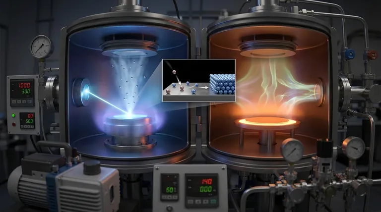
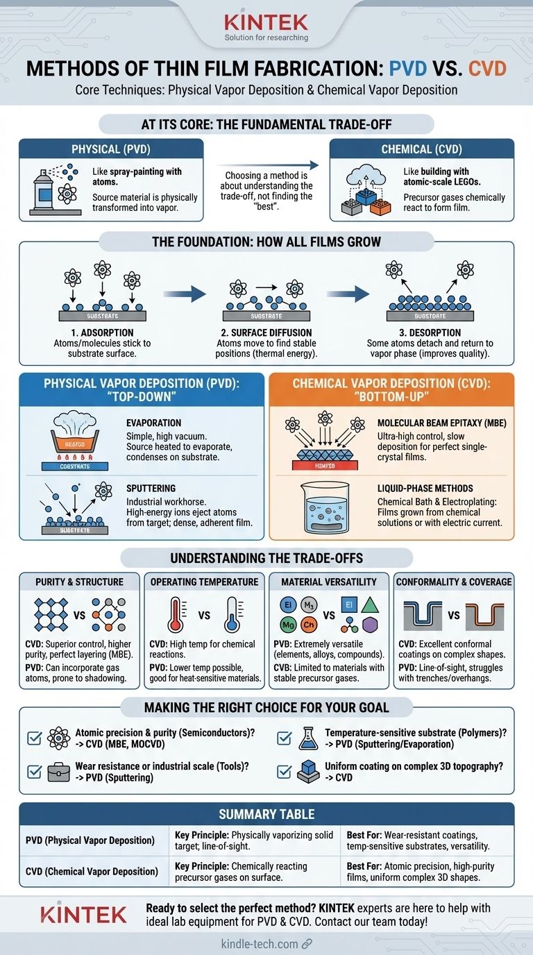
At its core, thin film fabrication is accomplished through two primary families of techniques: Physical Vapor Deposition (PVD) and Chemical Vapor Deposition (CVD). In PVD, a solid or liquid source material is physically transformed into a vapor—by heating or ion bombardment—which then condenses onto a substrate as a thin film. In contrast, CVD uses precursor gases that chemically react on a substrate's surface to form the film, building it up molecule by molecule.
Choosing a fabrication method is not about finding the "best" technique, but about understanding the fundamental trade-off. Physical methods are like spray-painting with atoms, while chemical methods are like building with atomic-scale LEGOs from a cloud of gas. Each is suited for different materials, desired properties, and applications.
The Foundation: How All Films Grow
Before comparing specific methods, it's critical to understand the three universal steps of film growth that every technique must manage. The quality of the final film depends entirely on controlling these phenomena at the atomic level.
### The Arrival: Adsorption
Adsorption is the first step, where atoms or molecules from the vapor phase stick to the substrate surface. For a film to grow, the deposition rate (controlled by the method) must be greater than the rate at which atoms might bounce off.
### The Movement: Surface Diffusion
Once atoms have landed on the surface, they don't immediately lock into place. They possess thermal energy, allowing them to move across the surface in a process called surface diffusion. This movement is crucial for finding and settling into a stable, low-energy position within the film's crystalline structure, which leads to a higher-quality, more ordered film.
### The Opposite: Desorption
Desorption is the process where an adsorbed atom detaches from the surface and returns to the vapor phase. While it seems counterproductive, some level of desorption can actually improve film quality by allowing weakly bonded or improperly placed atoms to leave, promoting a more uniform structure.
Physical Vapor Deposition (PVD): The "Top-Down" Approach
PVD techniques take a bulk source material (the "target") and physically eject its atoms, which then travel through a low-pressure environment and deposit onto the substrate. This is a line-of-sight process, much like spray painting.
### Evaporation
This is one of the simplest PVD methods. In a high vacuum, the source material is heated until it evaporates (or sublimates). These vaporized atoms travel in a straight line until they strike the cooler substrate, where they condense to form a film. It is relatively simple but offers less control over film structure than other methods.
### Sputtering
Sputtering is an industrial workhorse. In this method, a target of the source material is bombarded with high-energy ions (usually an inert gas like Argon). This bombardment acts like an atomic-scale sandblaster, physically knocking atoms off the target. These "sputtered" atoms then deposit onto the substrate, forming a dense and strongly adhered film.
Chemical Vapor Deposition (CVD): The "Bottom-Up" Approach
CVD builds a film from the ground up using chemical reactions. One or more volatile precursor gases are introduced into a reaction chamber. When these gases come into contact with a heated substrate, they react or decompose, leaving behind a solid film of the desired material.
### Molecular Beam Epitaxy (MBE)
MBE is a highly sophisticated, ultra-high-vacuum technique that offers the ultimate control over film growth. It involves directing beams of atoms or molecules at a heated, crystalline substrate. Deposition is so slow and precise—often less than one atomic layer per second—that it allows for the growth of perfect, single-crystal films (epitaxy). While sometimes classified as a PVD method due to its physical transport, its use of molecular sources and high-purity growth aligns with chemical principles.
### Liquid-Phase Chemical Methods
While most PVD and CVD methods occur in a vacuum or gas phase, films can also be grown from a liquid solution.
- Chemical Bath Deposition: The substrate is simply immersed in a chemical solution containing the necessary ions, which slowly precipitate onto the surface to form a solid film.
- Electroplating: This method uses an electric current passed through a solution (the electrolyte) to deposit material from a source (the anode) onto the substrate (the cathode).
Understanding the Trade-offs
The choice between PVD and CVD is dictated by the requirements of the final film and practical constraints like cost and substrate material.
### Purity and Structure Control
CVD generally offers superior control over film purity and crystalline structure. Because it's a chemical process, impurities can be more easily eliminated, and techniques like MBE enable perfect atomic layering. PVD films can sometimes incorporate gas atoms from the chamber and are prone to "shadowing" effects on complex-shaped parts.
### Operating Temperature
CVD typically requires high substrate temperatures to drive the necessary chemical reactions on the surface. PVD can often be performed at much lower temperatures, making it the ideal choice for coating heat-sensitive materials like plastics or pre-fabricated electronics.
### Material Versatility
PVD is extremely versatile and can be used to deposit almost any material, including elements, alloys, and compounds that are difficult to vaporize chemically. CVD is limited to materials for which suitable, stable, and often expensive precursor gases can be synthesized.
### Conformality and Coverage
CVD excels at creating conformal coatings—films that uniformly cover even highly complex, non-flat surfaces. Because the precursor gases can flow into and react inside small features, coverage is excellent. Line-of-sight PVD struggles with this, often leaving trenches and overhangs poorly coated.
Making the Right Choice for Your Goal
Selecting a fabrication method requires balancing the desired film properties with the realities of the material and application.
- If your primary focus is atomic-level precision and purity for advanced semiconductors: CVD techniques like MBE or MOCVD are the industry standard.
- If your primary focus is wear-resistant or decorative coatings on tools or parts at an industrial scale: PVD methods like sputtering provide excellent adhesion, high deposition rates, and material flexibility.
- If your primary focus is coating a temperature-sensitive substrate like a polymer: A low-temperature PVD process like sputtering or evaporation is the most practical solution.
- If your primary focus is achieving a uniform coating over a complex 3D topography: A CVD process is required for its superior conformality.
By understanding the fundamental principles of physical transport versus chemical reaction, you can confidently select the fabrication method that best aligns with your technical and economic goals.
Summary Table:
| Method | Key Principle | Best For |
|---|---|---|
| PVD (Physical Vapor Deposition) | Physically vaporizing a solid target; line-of-sight deposition. | Wear-resistant coatings, temperature-sensitive substrates, material versatility. |
| CVD (Chemical Vapor Deposition) | Chemically reacting precursor gases on a substrate surface. | Atomic-level precision, high-purity films, uniform coating on complex 3D shapes. |
Ready to select the perfect thin film fabrication method for your project? The experts at KINTEK are here to help. We specialize in providing the ideal lab equipment and consumables for both PVD and CVD processes, ensuring you achieve the precise film properties your research or production demands. Contact our team today to discuss your specific application and material goals!
Visual Guide
Related Products
- Inclined Rotary Plasma Enhanced Chemical Vapor Deposition PECVD Equipment Tube Furnace Machine
- HFCVD Machine System Equipment for Drawing Die Nano-Diamond Coating
- 915MHz MPCVD Diamond Machine Microwave Plasma Chemical Vapor Deposition System Reactor
- Vacuum Hot Press Furnace Machine for Lamination and Heating
- 1200℃ Split Tube Furnace with Quartz Tube Laboratory Tubular Furnace
People Also Ask
- What are the process capabilities of ICPCVD systems? Achieve Low-Damage Film Deposition at Ultra-Low Temperatures
- What is the process of PECVD in semiconductor? Enabling Low-Temperature Thin Film Deposition
- How do PECVD systems improve DLC coatings on implants? Superior Durability and Biocompatibility Explained
- Can plasma enhanced CVD deposit metals? Why PECVD is rarely used for metal deposition
- Why is a Matching Network Indispensable in RF-PECVD for Siloxane Films? Ensure Stable Plasma and Uniform Deposition
