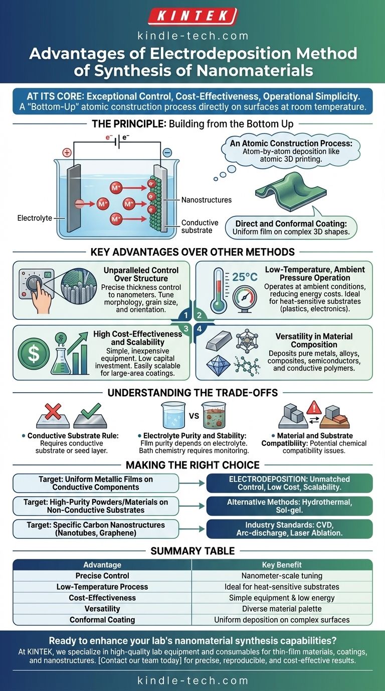
At its core, the electrodeposition method for synthesizing nanomaterials offers exceptional control, cost-effectiveness, and operational simplicity. Unlike high-energy methods, it allows for the precise, atom-by-atom construction of nanostructures directly onto a surface at room temperature, using relatively simple and inexpensive equipment.
The primary advantage of electrodeposition is its ability to create uniform, adherent thin films and nanostructures with precise thickness control directly on conductive substrates, all while operating under ambient temperature and pressure. This makes it a highly efficient and scalable "bottom-up" manufacturing technique.
The Principle: Building from the Bottom Up
Electrodeposition is an electrochemical process where a solid material is deposited onto a conductive surface (the cathode) from a solution containing its ions (the electrolyte). By applying a voltage, ions are driven to the surface, where they gain electrons and are reduced to their solid, metallic state, forming a thin film.
An Atomic Construction Process
Think of electrodeposition as an atomic-level form of 3D printing. The ions in the solution are the "ink," and the applied electrical current or voltage dictates the speed and precision with which this ink is deposited onto the substrate.
This is a classic "bottom-up" approach, meaning the final material is built atom by atom. This contrasts sharply with "top-down" methods that start with a bulk material and carve it down to the nanoscale.
Direct and Conformal Coating
Because the process is driven by an electric field in a liquid medium, electrodeposition can coat complex, three-dimensional shapes with a uniform film. The material deposits on any conductive part of the substrate that the electrolyte can reach, a significant advantage over line-of-sight methods like evaporation or sputtering.
Key Advantages Over Other Methods
When compared to techniques like Chemical Vapor Deposition (CVD), sol-gel, or hydrothermal synthesis, electrodeposition presents a unique set of compelling benefits for specific applications.
Unparalleled Control Over Structure
By carefully manipulating parameters like voltage, current density, and deposition time, you can precisely control the film thickness down to the nanometer scale. Furthermore, adjusting additives and bath chemistry allows for tuning the material's morphology, such as grain size, crystal orientation, and porosity.
Low-Temperature, Ambient Pressure Operation
One of the most significant advantages is that electrodeposition typically occurs at or near room temperature and pressure. This drastically reduces energy costs and eliminates the need for expensive high-temperature furnaces or vacuum chambers required for methods like CVD or laser ablation. It also makes it possible to coat heat-sensitive substrates, such as plastics or organic electronics.
High Cost-Effectiveness and Scalability
The required equipment is remarkably simple: a power supply, a beaker, electrodes, and the electrolyte solution. This low capital investment makes it accessible for both research and industrial-scale production. Scaling up the process for large-area coatings is often a matter of using a larger bath and substrate, making it highly economical.
Versatility in Material Composition
While excellent for pure metals, electrodeposition is also highly effective for creating alloys by using an electrolyte with multiple types of metal ions. It can also be used to synthesize composite materials, semiconductor compounds, and conductive polymers, offering a broad material palette.
Understanding the Trade-offs and Limitations
No method is perfect. Being objective means recognizing where electrodeposition falls short or presents challenges.
The Conductive Substrate Rule
The most fundamental limitation is the requirement for a conductive substrate. While non-conductive surfaces can be used after pre-treating them with a thin conductive seed layer, this adds an extra step and complexity not present in methods like sol-gel, which can easily coat insulators like glass or ceramics directly.
Electrolyte Purity and Stability
The final film's purity is entirely dependent on the purity of the electrolyte bath. Any impurities in the solution can be co-deposited, potentially degrading the nanomaterial's electrical, mechanical, or optical properties. The bath chemistry can also change over time, requiring careful monitoring and maintenance for consistent results.
Material and Substrate Compatibility
There can be chemical compatibility issues between the electrolyte solution and the substrate. Some aggressive electrolyte formulations may corrode or damage the substrate material you intend to coat.
Making the Right Choice for Your Goal
Selecting a synthesis method requires matching its strengths to your project's specific requirements for material, structure, and cost.
- If your primary focus is creating highly uniform, thin metallic films on a conductive component: Electrodeposition offers an unmatched combination of control, low cost, and scalability.
- If your primary focus is synthesizing high-purity freestanding powders or materials on non-conductive substrates: Methods like hydrothermal synthesis or sol-gel often provide more flexibility.
- If your primary focus is creating specific carbon nanostructures like nanotubes or graphene: Chemical Vapor Deposition (CVD), arc-discharge, or laser ablation are the industry-standard techniques.
By understanding these fundamental trade-offs, you can confidently select the synthesis technique that best aligns with your material, substrate, and performance requirements.
Summary Table:
| Advantage | Key Benefit |
|---|---|
| Precise Control | Nanometer-scale thickness & morphology tuning |
| Low-Temperature Process | Room temperature operation, ideal for heat-sensitive substrates |
| Cost-Effectiveness | Simple equipment, low energy use, and easy scalability |
| Versatility | Capable of depositing metals, alloys, composites, and polymers |
| Conformal Coating | Uniform deposition on complex 3D conductive surfaces |
Ready to enhance your lab's nanomaterial synthesis capabilities?
At KINTEK, we specialize in providing high-quality lab equipment and consumables tailored to your research needs. Whether you are developing new thin-film materials, coatings, or nanostructures, our solutions can help you achieve precise, reproducible, and cost-effective results.
Let's discuss how our expertise can support your projects. Contact our team today to find the perfect equipment for your electrodeposition and nanomaterial synthesis workflows!
Visual Guide
Related Products
- Chemical Vapor Deposition CVD Equipment System Chamber Slide PECVD Tube Furnace with Liquid Gasifier PECVD Machine
- Customer Made Versatile CVD Tube Furnace Chemical Vapor Deposition Chamber System Equipment
- Electron Beam Evaporation Coating Oxygen-Free Copper Crucible and Evaporation Boat
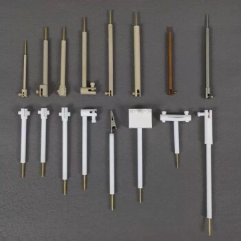
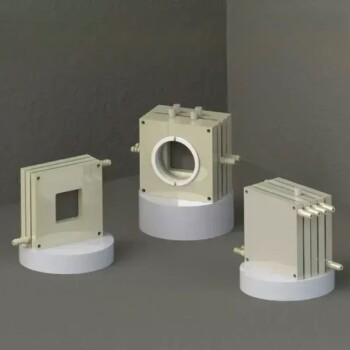
- Electrode Fixture for Electrochemical Experiments
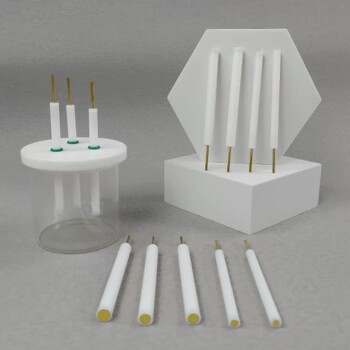
- Rotating Platinum Disk Electrode for Electrochemical Applications
People Also Ask
- Why is Chemical Vapor Deposition (CVD) equipment uniquely suited for constructing hierarchical superhydrophobic structures?
- What happens during deposition chemistry? Building Thin Films from Gaseous Precursors
- What are the advantages of chemical vapor deposition? Achieve Superior Thin Films for Your Lab
- How are carbon nanotubes grown? Master Scalable Production with Chemical Vapor Deposition
- What is the chemical vapor deposition growth process? Build Superior Thin Films from the Atom Up