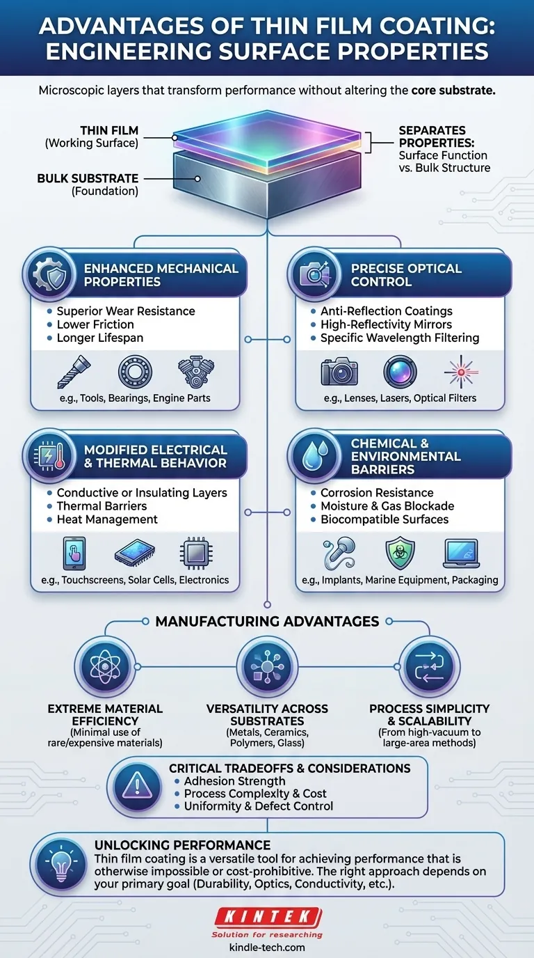
At its core, thin film coating is a technology used to apply a microscopic layer of material onto a surface, fundamentally altering its properties without changing the underlying substrate. The primary advantages are the ability to add new functions—like wear resistance, optical filtering, or electrical conductivity—to a bulk material with extreme precision and minimal use of resources.
Thin film coatings are not just protective layers; they are a strategic method for engineering surface properties. They enable performance and functionality that the base material alone cannot achieve, often with significant gains in efficiency and durability.
How Thin Films Transform a Surface
To understand the advantages, it's crucial to first understand the principle. A thin film acts as the new "working surface" of an object, while the bulk material provides the structural foundation.
Defining "Thin" Film
A thin film is a layer of material ranging from fractions of a nanometer to several micrometers in thickness. At this scale, the properties of the film can be dramatically different from the same material in bulk form.
The Principle of Surface Engineering
This technology separates the desired surface properties (e.g., hardness, reflectivity) from the required bulk properties (e.g., strength, weight, cost). You can use a cheap, lightweight plastic for a device's body but apply a thin film to give its lens a scratch-resistant, anti-reflective surface.
Key Performance Advantages
The true power of thin films lies in the wide range of functional properties they can introduce to a substrate.
Enhanced Mechanical Properties
By depositing very hard materials like titanium nitride (TiN) or diamond-like carbon (DLC), you can drastically improve a component's surface. This leads to superior wear resistance, lower friction, and a longer operational lifespan for tools, bearings, and engine parts.
Precise Control of Light
Thin films are essential in optics. By stacking multiple layers of specific materials and thicknesses, engineers can create highly specialized coatings. These include anti-reflection coatings for camera lenses, high-reflectivity mirrors for lasers, and band-pass filters that only allow specific wavelengths of light to pass through.
Modified Electrical and Thermal Behavior
Thin films can be used to add electrical functionality. Transparent conductive oxides (like ITO) are used in touchscreens and solar cells. Conversely, insulating films like silicon dioxide are fundamental to manufacturing microchips. They can also act as thermal barriers, managing heat in high-performance electronics.
Chemical and Environmental Barriers
A dense, non-porous thin film can seal a substrate from its environment. This is critical for preventing corrosion on metals, blocking moisture permeation in electronics, and creating biocompatible surfaces for medical implants.
Understanding the Manufacturing Advantages
Beyond performance, the methods used to create thin films offer their own set of benefits.
Extreme Material Efficiency
Because the layers are incredibly thin, the amount of material required is minuscule. This makes it economically feasible to use expensive or rare materials, like gold or platinum, to achieve a desired surface effect without making the entire object out of them.
Versatility Across Substrates and Scales
Thin films can be applied to a vast range of substrates, including metals, ceramics, polymers, and glass. The processes for creating them can be adapted for different needs. For example, some methods excel at coating complex 3D shapes, while others are designed for massive, flat surfaces like architectural glass.
Process Simplicity and Low Temperatures
While some methods require high vacuum and temperature, others like the sol-gel process are known for their relative simplicity. These techniques allow for excellent film uniformity over large areas and can often be performed at low temperatures, making them suitable for coating heat-sensitive substrates like plastics.
Critical Trade-offs and Considerations
Thin film technology is powerful but not without its challenges. Objectivity requires acknowledging them.
The Challenge of Adhesion
A coating is only as effective as its bond to the substrate. Poor adhesion can cause the film to peel, flake, or delaminate, rendering it useless. Achieving a strong, durable bond is a critical and often complex aspect of the coating process.
Process Complexity and Cost
High-performance films created with processes like Physical Vapor Deposition (PVD) or Chemical Vapor Deposition (CVD) require sophisticated, high-vacuum equipment. The initial capital investment and operational complexity for these systems can be substantial.
Uniformity and Defect Control
Microscopic defects like pinholes, cracks, or variations in thickness can compromise the entire function of the film. Maintaining strict process control to ensure uniformity and minimize defects is essential, especially in high-precision applications like optics and semiconductors.
Making the Right Choice for Your Goal
Selecting the right thin film approach depends entirely on your primary objective.
- If your primary focus is mechanical durability: Investigate hard coatings like TiN or DLC, typically applied via PVD, as they offer the best wear resistance for tools and components.
- If your primary focus is optical precision: Focus on dielectric or metallic stacks applied via methods like sputtering or evaporation, which allow for nanometer-level thickness control.
- If your primary focus is cost-effective, large-area coverage: Explore atmospheric pressure techniques like the sol-gel method or spray pyrolysis, especially if extreme performance is not the top priority.
- If your primary focus is creating a conductive, transparent layer: Your best option will likely be sputtered Transparent Conductive Oxides (TCOs) like Indium Tin Oxide (ITO).
Ultimately, thin film coating is a versatile and powerful tool for unlocking material performance that would otherwise be impossible or cost-prohibitive.
Summary Table:
| Advantage Category | Key Benefits |
|---|---|
| Mechanical Properties | Wear resistance, lower friction, longer lifespan |
| Optical Control | Anti-reflection, high reflectivity, precise filtering |
| Electrical & Thermal | Conductive or insulating layers, thermal management |
| Chemical & Environmental | Corrosion resistance, moisture barriers, biocompatibility |
| Manufacturing Efficiency | Material efficiency, versatility, process simplicity |
Ready to engineer superior surface properties for your components?
KINTEK specializes in advanced thin film coating solutions and lab equipment. Whether you need to enhance wear resistance, achieve precise optical filtering, or add electrical functionality to your substrates, our expertise can help you select the right coating process and materials for your specific application.
Contact our experts today to discuss how our thin film technologies can improve your product's performance, durability, and efficiency.
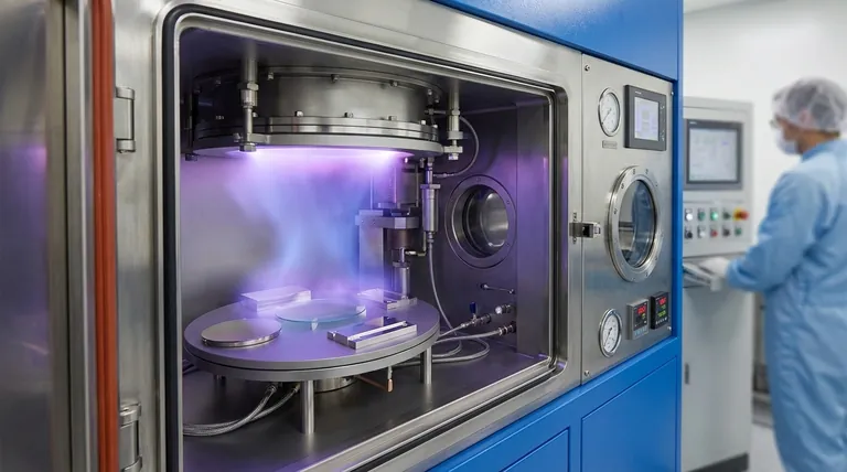
Visual Guide
Related Products
- Aluminized Ceramic Evaporation Boat for Thin Film Deposition
- Electron Beam Evaporation Coating Oxygen-Free Copper Crucible and Evaporation Boat
- Tungsten Evaporation Boat for Thin Film Deposition
- Molybdenum Tungsten Tantalum Evaporation Boat for High Temperature Applications
- Aluminum-Plastic Flexible Packaging Film for Lithium Battery Packaging
People Also Ask
- Why are high-purity ceramic boats used for lignin activation? Ensure Purity & Thermal Stability
- What is the widely used boat made of in thermal evaporation? Choosing the Right Material for High-Purity Deposition
- Why is an alumina boat selected for catalyst precursors? Ensure Sample Purity at 1000 °C
- What is thin film deposition? Unlock Advanced Surface Engineering for Your Materials
- What are the applications of thin films deposition? Unlock New Possibilities for Your Materials


