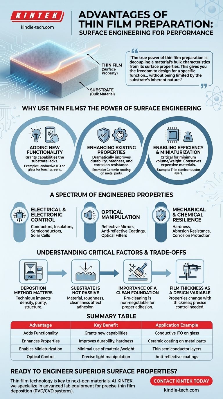
At its core, thin film preparation is about precision engineering at the atomic level. The primary advantages are the ability to fundamentally alter a material's surface to give it new or enhanced properties—such as electrical conductivity, optical filtering, or extreme hardness—that the underlying material (the substrate) lacks. This allows for the creation of high-performance components that are efficient in their use of materials, weight, and volume.
The true power of thin film preparation is decoupling a material's bulk characteristics from its surface properties. This gives you the freedom to design for a specific function—like conductivity, durability, or optical performance—without being limited by the substrate's inherent nature.
Why Not Just Use a Different Bulk Material? The Power of Surface Engineering
The decision to use a thin film is a strategic one. It is often driven by the need to combine the best properties of two different materials: the structural integrity or low cost of a substrate with the high-performance surface of a deposited film.
Adding New Functionality
Often, the goal is to grant a material a capability it simply does not have. A thin film can add a functional layer that performs a task the bulk substrate cannot.
For example, a thin layer of a conductive material like indium tin oxide (ITO) can be deposited onto glass, making the surface electrically conductive while remaining optically transparent. The glass provides the structure, and the film provides the function.
Enhancing Existing Properties
In other cases, a thin film is used to dramatically improve a property the substrate already possesses. This is common for increasing the durability or resilience of a component.
A metal part might be coated with a thin ceramic film to make it significantly more resistant to scratches, wear, and corrosion, extending its operational life far beyond that of the uncoated metal.
Enabling Efficiency and Miniaturization
Thin films are, by definition, exceptionally thin. This provides a significant advantage in applications where minimum volume and weight are critical design constraints.
Furthermore, it allows for the conservation of scarce or expensive materials. A tiny amount of a precious material like gold or platinum can be used as a functional film, rather than constructing the entire part from it.
A Spectrum of Engineered Properties
The specific advantage of a thin film is determined by its composition and structure. The technology provides a wide palette of characteristics that can be engineered for a specific outcome.
Electrical and Electronic Control
Thin films are foundational to the modern electronics industry. They can be designed to control the flow of electricity with incredible precision.
Properties include creating conductors for circuits, insulators to prevent shorts, semiconductors for transistors, and specialized layers for solar cells that convert light into energy.
Optical Manipulation
By controlling a film's thickness and refractive index, you can precisely manage how it interacts with light.
This enables the creation of highly reflective mirrors, anti-reflective coatings for lenses and displays, and optical filters that transmit or block specific wavelengths of light.
Mechanical and Chemical Resilience
Thin films can serve as a protective shield for the underlying substrate, creating a barrier against the physical and chemical environment.
This is used to engineer surfaces with exceptional hardness, abrasion resistance, and protection against corrosion or chemical attack.
Understanding the Trade-offs and Critical Factors
Achieving these advantages is not automatic. The success of a thin film application depends on careful control over several key factors. Mismanaging them can lead to poor performance and device failure.
The Deposition Method Matters
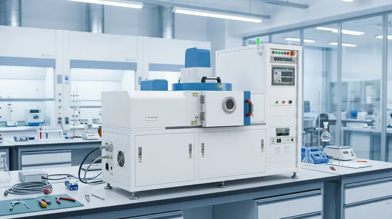
The technique used to create the film—such as Physical Vapor Deposition (PVD) or Chemical Vapor Deposition (CVD)—has a profound impact on the film’s final properties, including its density, purity, and structure. The right choice depends entirely on the desired material and application.
The Substrate Is Not Passive
The properties of the thin film are directly influenced by the substrate it is deposited on. Factors like the substrate's material, surface roughness, and cleanliness determine how well the film will adhere and perform.
The Importance of a Clean Foundation
Proper pre-cleaning of the substrate is non-negotiable. Contaminants can prevent proper adhesion, leading to film delamination. They can also create inconsistencies in the film's density and uniformity, degrading its optical or electrical performance and lowering manufacturing yield.
Film Thickness as a Design Variable
The properties of a material in thin film form can be drastically different from its bulk form. Furthermore, these properties can change significantly with the film's thickness. Thickness is a critical design parameter that must be precisely controlled.
Applying This to Your Project
The decision to leverage thin film technology should be guided by your primary objective.
- If your primary focus is novel electronics or optics: Leverage the ability to create nanostructured coatings that manipulate electrons and photons with unparalleled precision.
- If your primary focus is improving a physical product: Use films to add high-value properties like wear resistance, corrosion protection, or optical coatings to cost-effective substrates.
- If your primary focus is manufacturing efficiency: Capitalize on the minimal use of expensive materials and the low added weight to create economical and lightweight components.
Ultimately, mastering thin film technology empowers you to create materials that are precisely tailored to their intended function.
Summary Table:
| Advantage | Key Benefit | Application Example |
|---|---|---|
| Adds Functionality | Grants new capabilities to a substrate | Conductive ITO coating on glass for touchscreens |
| Enhances Properties | Improves durability, hardness, corrosion resistance | Ceramic coating on metal parts for wear resistance |
| Enables Miniaturization | Minimal use of material, weight, and volume | Thin semiconductor layers in microchips and solar cells |
| Optical Control | Precise manipulation of light (anti-reflective, filtering) | Anti-reflective coatings on lenses and displays |
Ready to Engineer Superior Surface Properties?
Thin film technology is key to developing next-generation materials with tailored electrical, optical, and mechanical performance. At KINTEK, we specialize in providing the advanced lab equipment and consumables—including PVD and CVD systems—necessary for precise thin film deposition.
Whether you are developing novel electronics, enhancing product durability, or optimizing manufacturing efficiency, our solutions help you achieve the high-purity, uniform coatings required for success.
Contact KINTEK today to discuss how our expertise in lab equipment can support your thin film preparation projects and bring your high-performance material designs to life.
Visual Guide
Related Products
- Aluminized Ceramic Evaporation Boat for Thin Film Deposition
- Molybdenum Tungsten Tantalum Evaporation Boat for High Temperature Applications
- Electron Beam Evaporation Coating Oxygen-Free Copper Crucible and Evaporation Boat
- Thin-Layer Spectral Electrolysis Electrochemical Cell
- Aluminum-Plastic Flexible Packaging Film for Lithium Battery Packaging
People Also Ask
- Why is an alumina boat selected for catalyst precursors? Ensure Sample Purity at 1000 °C
- What are the alternatives to sputtering? Choose the Right Thin Film Deposition Method
- What is the chemical method for thin film deposition? Build Films from the Molecular Level Up
- What are the applications of thin films deposition? Unlock New Possibilities for Your Materials
- Why are high-purity ceramic boats used for lignin activation? Ensure Purity & Thermal Stability


