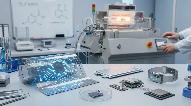
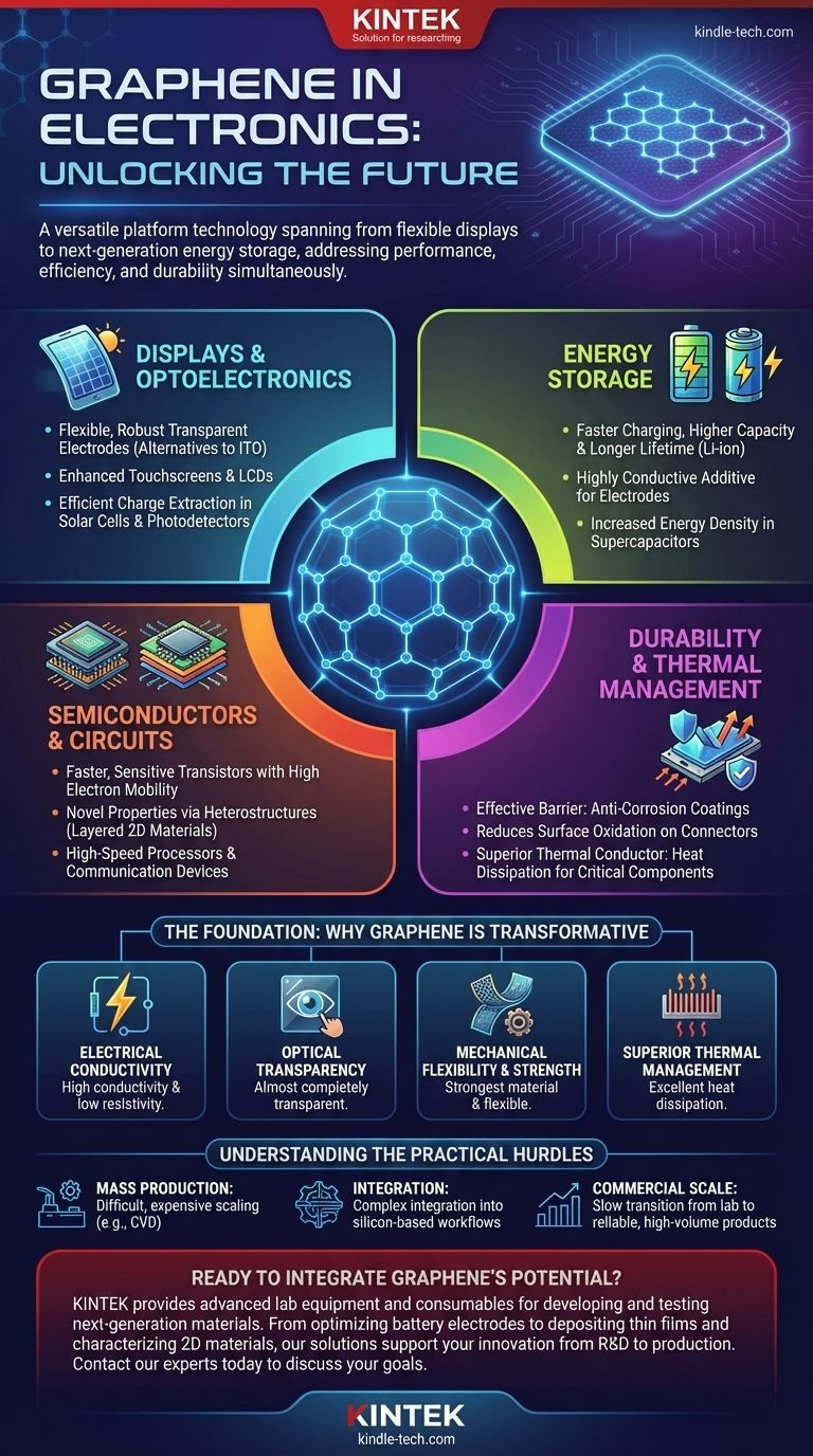
In the field of electronics, graphene is not a single-solution material but a versatile platform technology with applications spanning from transparent and flexible displays to next-generation energy storage. Its primary uses are found in optoelectronics (like solar cells and touchscreens), faster transistors and sensors, enhanced lithium-ion batteries and supercapacitors, and protective coatings that improve device durability and thermal management.
Graphene's true significance in electronics comes from its unique combination of properties. Its ability to be simultaneously conductive, transparent, flexible, and strong allows it to solve multiple engineering challenges at once, improving performance, efficiency, and longevity in a wide range of components.
The Foundation: Why Graphene is Transformative
Graphene’s potential stems from a set of physical properties that are rarely found together in a single material. Understanding these is key to grasping its applications.
Unmatched Electrical Conductivity
Graphene possesses exceptionally high electrical conductivity and low resistivity. This makes it a prime candidate for creating more efficient circuits and interconnections in microelectronics.
This property is especially valuable in thin-films and as a conductive anode material in organic photovoltaic (OPV) cells, where efficient charge transport is critical.
Optical Transparency
Despite being made of carbon, a single layer of graphene is almost completely transparent. This, combined with its conductivity, is a revolutionary combination.
It enables the creation of transparent conductive films, which are essential components in touchscreens, liquid crystal displays (LCDs), and light-emitting diodes (LEDs).
Mechanical Flexibility and Strength
Graphene is one of the strongest materials ever measured, yet it remains incredibly flexible. This allows it to be incorporated into non-rigid electronics.
This opens the door for flexible displays, wearable sensors, and bendable solar cells that can be integrated into clothing or other unconventional surfaces.
Superior Thermal Management
The material is an excellent thermal conductor, meaning it can dissipate heat very effectively. In densely packed modern electronics, managing heat is a primary engineering challenge.
Graphene can be used as a conductive barrier or coating that draws heat away from critical components like processors or batteries, improving performance and preventing degradation.
Key Application Areas in Modern Electronics
Based on its core properties, graphene is being applied to solve specific problems across the electronics industry, from consumer devices to high-end industrial systems.
Enhancing Displays and Optoelectronics
Graphene’s use as a transparent electrode is one of its most promising applications. It offers a flexible and more robust alternative to the brittle Indium Tin Oxide (ITO) currently used in most touchscreens.
In solar cells and photodetectors, its transparency allows light to pass through to the active layers while its conductivity efficiently extracts the generated current.
Advancing Energy Storage
In lithium-ion batteries, graphene improves charging speed, capacity, and operational lifetime. It acts as a highly conductive additive in electrodes, allowing for faster ion transport.
For supercapacitors, graphene's incredibly high specific surface area enables the storage of a much greater electrical charge, leading to devices with higher energy density.
Improving Semiconductors and Circuits
Graphene is used to design faster and more sensitive transistors. Its high electron mobility allows for quicker switching times, a key factor for next-generation processors and communication devices.
It is also used to create heterostructures, which are layered stacks of different 2D materials. These structures unlock novel electronic and optoelectronic properties not found in individual materials.
Increasing Durability and Lifespan
As an ultra-thin coating, graphene provides an effective barrier against environmental factors. It can be used as an anti-corrosion paint or a direct coating on electronic components.
Its inert nature reduces surface oxidation on parts like pin connectors, extending the reliable life of electronic hardware.
Understanding the Practical Hurdles
While graphene's properties are exceptional, its widespread adoption faces significant real-world challenges that are important to acknowledge.
The Challenge of Mass Production
Producing large sheets of high-quality, defect-free graphene is difficult and expensive. Methods like Chemical Vapor Deposition (CVD) are effective but scaling them to meet industrial demand at a low cost remains a primary obstacle.
Integration with Existing Manufacturing
The electronics industry is built around silicon-based fabrication processes. Integrating a new material like graphene into these highly optimized, multi-billion-dollar workflows is a complex and costly engineering endeavor.
From Lab to Commercial Scale
Many of graphene's most exciting applications are still in the research and development phase. While proof-of-concept devices exist, moving to reliable, high-volume commercial products is a slow and deliberate process.
Making the Right Choice for Your Goal
When evaluating graphene, it is crucial to align its potential with a specific engineering objective.
- If your primary focus is performance and speed: Look to graphene's applications in high-frequency transistors, optical modulators for 6G, and low-resistivity interconnections.
- If your primary focus is energy efficiency and storage: Concentrate on its use in enhancing Li-ion batteries, developing high-density supercapacitors, and improving transparent electrodes in solar cells.
- If your primary focus is durability and device lifespan: Consider its role in anti-corrosion coatings, thermal management films, and protective layers for sensitive components.
- If your primary focus is developing next-generation form factors: Explore its potential in creating flexible displays, wearable bio-sensors, and conformable electronics.
Ultimately, graphene's value lies in its unique capacity to address performance, efficiency, and durability simultaneously, creating a pathway for a new generation of electronic devices.
Summary Table:
| Application Area | Key Benefit of Graphene |
|---|---|
| Displays & Optoelectronics | Transparent, flexible electrodes for touchscreens and solar cells. |
| Energy Storage | Faster charging, higher capacity in batteries and supercapacitors. |
| Semiconductors & Circuits | High-speed transistors and novel heterostructures for advanced chips. |
| Durability & Thermal Management | Protective anti-corrosion coatings and superior heat dissipation. |
Ready to integrate graphene's potential into your electronic components or lab research? KINTEK specializes in providing advanced lab equipment and consumables essential for developing and testing next-generation materials like graphene. Whether you're optimizing battery electrodes, depositing thin films, or characterizing 2D materials, our solutions support your innovation from R&D to production. Contact our experts today to discuss how we can help you achieve superior performance and durability.
Visual Guide
Related Products
- Graphite Vacuum Furnace High Thermal Conductivity Film Graphitization Furnace
- Carbon Graphite Plate Manufactured by Isostatic Pressing Method
- Graphite Disc Rod and Sheet Electrode Electrochemical Graphite Electrode
- High Purity Pure Graphite Crucible for Electron Beam Evaporation
- Ultra-High Temperature Graphite Vacuum Graphitization Furnace
People Also Ask
- What are the disadvantages of graphite furnace? Key Limitations and Operational Costs
- What is the use of graphite furnace? Achieve Extreme-Temperature Processing for Advanced Materials
- What is the temperature of a graphite furnace? Achieve Extreme Heat Up to 3000°C
- What is the disadvantage of graphite furnace? Managing Reactivity and Contamination Risks
- What is a graphite furnace? Unlock Extreme Temperatures and Purity for Advanced Materials