The fundamental challenge of graphene synthesis is the inherent and unavoidable trade-off between quality, quantity, and cost. While methods exist to produce pristine, single-atom-thick sheets, they are not scalable or cost-effective for mass production. Conversely, methods that yield large quantities are cheaper but inevitably produce graphene with significant structural defects, compromising its "wonder material" properties.
The central dilemma in the field is that no single synthesis method can simultaneously deliver high-quality, large-scale, and low-cost graphene. Your choice of method is therefore not a search for the "best" process, but a strategic compromise based on your specific application and budget.
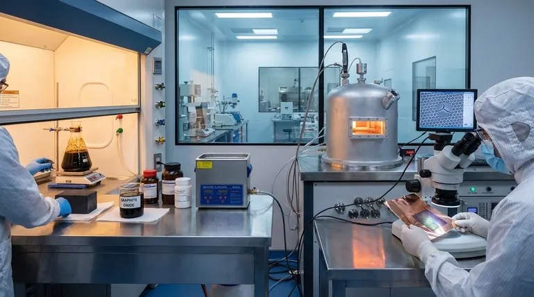
The Two Philosophies of Graphene Production
At a high level, all synthesis techniques fall into two categories, each with its own distinct set of challenges. This division represents the core tension in graphene manufacturing.
Top-Down: Starting Big and Breaking It Down
This approach begins with bulk graphite—essentially a stack of countless graphene layers—and aims to separate it into individual sheets. These methods are generally better suited for producing large quantities.
Bottom-Up: Building from the Atom Up
This approach constructs the graphene lattice atom by atom on a catalytic surface. These methods are prized for their ability to create high-quality, continuous sheets of graphene ideal for high-performance applications.
Challenges of Top-Down Synthesis (The 'Bulk' Approach)
The primary goal here is scale, but this comes at the cost of control and purity.
Chemical Oxidation-Reduction
This is the most common method for industrial-scale production. Graphite is treated with strong oxidizing acids, which force the layers apart by intercalating oxygen-containing functional groups, creating graphene oxide (GO).
The main challenge is that this process aggressively damages the carbon lattice. GO is an electrical insulator and must be "reduced" back into reduced graphene oxide (rGO), but this secondary process is imperfect and leaves behind vacancies and residual oxygen, degrading its electrical and thermal conductivity.
Liquid Phase Exfoliation
In this method, graphite is sonicated (agitated with high-frequency sound waves) in a specific solvent. The energy overcomes the forces holding the layers together, causing them to shear off.
The challenge is a lack of control and low yield of single-layer graphene. The output is a mixture of single-layer, few-layer, and even thick graphite flakes. Removing the solvent without causing the flakes to re-stack is also a significant hurdle.
Mechanical Exfoliation
This is the famous "Scotch tape" method that first isolated graphene. A piece of tape peels layers from a graphite crystal.
While it can produce incredibly high-quality, pristine flakes, the challenge is that it is entirely unscalable. Its yield is minuscule, making it suitable only for fundamental laboratory research, not for any commercial product.
Challenges of Bottom-Up Synthesis (The 'Precision' Approach)
These methods offer superior quality and control, but face major obstacles related to cost, complexity, and integration.
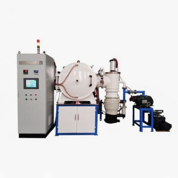
Chemical Vapor Deposition (CVD)
CVD is the leading technique for producing large-area, high-quality graphene films for electronics. A hydrocarbon gas (like methane) is introduced into a high-temperature furnace containing a copper or nickel foil. The catalyst breaks down the gas, and carbon atoms assemble into a graphene film on the metal's surface.
The single biggest challenge is the transfer process. The atom-thick graphene film must be moved from the metal growth foil to a target substrate (like silicon). This delicate step frequently introduces tears, wrinkles, folds, and contamination, which act as defects that ruin device performance.
Other major challenges include the high cost associated with high temperatures (~1000°C), vacuum systems, and the grain boundaries (defects) that form where individual graphene crystals meet as they grow.
Epitaxial Growth on Silicon Carbide (SiC)
This method involves heating a silicon carbide wafer to very high temperatures (above 1300°C). The silicon sublimates (evaporates) from the surface, leaving behind carbon atoms that rearrange themselves into a high-quality graphene layer.
The overwhelming challenge is the prohibitive cost of the SiC wafer itself. While this method brilliantly avoids the difficult transfer step of CVD, its expense limits its use to niche, high-performance applications where cost is a secondary concern.
Making the Right Choice for Your Goal
Navigating these challenges requires aligning your synthesis method with the non-negotiable requirements of your end-use.
- If your primary focus is high-performance electronics: CVD is the most viable path for large-area films, but you must dedicate significant resources to perfecting a clean, reliable transfer process.
- If your primary focus is bulk materials like composites, conductive inks, or coatings: Chemical oxidation to create rGO is the most pragmatic choice, as its scalability and low cost outweigh the lower electronic quality.
- If your primary focus is fundamental physics research: Mechanical exfoliation remains the gold standard for producing tiny, near-perfect flakes to study graphene's intrinsic properties.
Ultimately, successful graphene implementation is less about finding a perfect material and more about understanding the practical limitations of the material you can actually produce.
Summary Table:
| Synthesis Method | Primary Challenge | Best For |
|---|---|---|
| Chemical Oxidation-Reduction | Structural defects, poor conductivity | Bulk composites, conductive inks |
| Liquid Phase Exfoliation | Low single-layer yield, re-stacking | Dispersions, coatings |
| Mechanical Exfoliation | Unscalable, low yield | Fundamental research |
| Chemical Vapor Deposition (CVD) | Complex, defect-prone transfer | High-performance electronics |
| Epitaxial Growth on SiC | Prohibitive substrate cost | Niche high-performance applications |
Ready to Overcome Your Graphene Synthesis Challenges?
Navigating the trade-offs between quality, scale, and cost is complex, but you don't have to do it alone. KINTEK specializes in providing the precise lab equipment and consumables needed to optimize your graphene synthesis process, whether you're focused on high-performance electronics or scalable bulk materials.
We help you:
- Select the right synthesis method for your specific application and budget
- Source reliable CVD systems, furnaces, and transfer tools for high-quality graphene
- Access consumables for top-down methods like chemical exfoliation
- Improve yield and consistency with expert technical support
Let's discuss your graphene project and find the most effective path forward. Contact our experts today to explore how KINTEK's solutions can accelerate your research and development.
Visual Guide

Related Products
- Ultra-High Temperature Graphite Vacuum Graphitization Furnace
- Carbon Graphite Plate Manufactured by Isostatic Pressing Method
- High Purity Pure Graphite Crucible for Evaporation
- Graphite Vacuum Furnace High Thermal Conductivity Film Graphitization Furnace
- High Purity Pure Graphite Crucible for Electron Beam Evaporation
People Also Ask
- What is a graphite furnace? Unlock Extreme Temperatures and Purity for Advanced Materials
- What gas is used in graphite furnace? Maximize Accuracy with the Right Inert Gas
- Is a graphite melting point high or low? Discover Its Extreme Thermal Resilience
- What is the disadvantage of graphite furnace? Managing Reactivity and Contamination Risks
- What is the temperature of a graphite furnace? Achieve Extreme Heat Up to 3000°C