At its core, Chemical Vapor Deposition (CVD) is used across numerous high-technology fields. Its most prominent examples include the fabrication of thin films for the semiconductor industry to create integrated circuits, the production of high-purity synthetic diamonds for industrial and jewelry use, and the application of durable, wear-resistant coatings on tools and medical implants.
The key takeaway is that CVD is not a single product but a highly versatile platform technology. Its true value lies in its ability to construct solid materials atom-by-atom from a gaseous state, enabling the creation of ultra-pure, high-performance thin films that are essential for modern electronics, advanced materials, and biomedical devices.
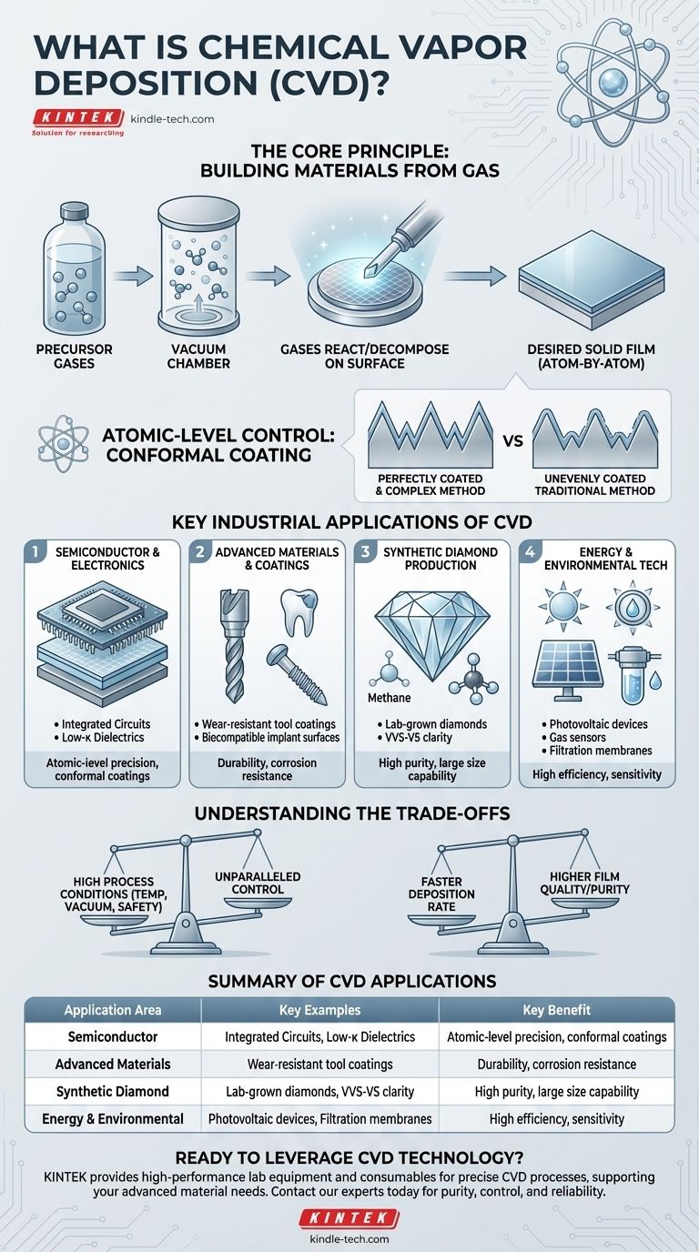
The Core Principle: Building Materials from Gas
What is Chemical Vapor Deposition?
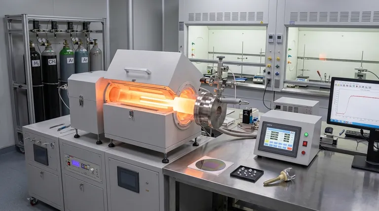
Chemical Vapor Deposition is a process where a substrate (the object to be coated) is exposed to one or more volatile precursor gases. These gases react or decompose on the substrate's surface to produce the desired solid material deposit, or film.
This method allows for building a material layer by layer, offering incredible control over its thickness, composition, and structure.
The Advantage of Atomic-Level Control
Because CVD builds films from the bottom up, it can create layers that are perfectly conformal, meaning they uniformly coat even the most complex and intricate surfaces. This is a capability that traditional coating techniques cannot easily replicate.
This precision is crucial for producing extremely thin, high-quality, and pure materials necessary for high-performance applications.
Key Industrial Applications of CVD
Semiconductor and Electronics Manufacturing
This is arguably the most significant application of CVD. It is fundamental to producing the layered, microscopic structures found in integrated circuits and circuit boards.
Specialized CVD techniques are used to deposit the various conductive, insulating (like low-κ dielectrics), and semiconducting films that form transistors and wiring on a silicon wafer.
Advanced Materials and Coatings
CVD is used to apply exceptionally hard and durable coatings to a variety of substrates. These wear-resistant coatings extend the life of cutting tools and industrial components.
Furthermore, its ability to create corrosion-resistant and biocompatible layers makes it invaluable for treating the surfaces of biomedical device implants, ensuring they function safely and effectively within the human body.
Synthetic Diamond Production
CVD is a leading method for growing high-quality, lab-grown diamonds. This process typically uses a mixture of hydrogen and a carbon-containing gas (like methane) at low pressure.
Compared to other methods, CVD allows for the production of large, high-clarity diamonds (VVS-VS clarity) without the metallic inclusions often found in high-pressure techniques.
Energy and Environmental Technology
The precision of CVD is leveraged in the production of photovoltaic devices, or solar cells, where thin films are required to efficiently convert sunlight into electricity.
It is also used to create specialized membrane coatings for advanced filtration systems, including water treatment and desalination, as well as in the fabrication of highly sensitive gas sensors.
Understanding the Trade-offs
Process Conditions and Complexity
While CVD offers unparalleled control, the processes often require high temperatures and vacuum conditions. This necessitates sophisticated, and often expensive, equipment.
The precursor gases used can also be highly toxic, flammable, or corrosive, requiring stringent safety protocols and handling procedures.
Deposition Rate vs. Film Quality
There is often a direct trade-off between the speed of the coating process and the quality of the resulting film.
Techniques designed for the highest-purity, most uniform films, such as Atomic Layer Deposition (a subtype of CVD), are often significantly slower than other methods. This makes process selection a critical decision based on the desired outcome and economic feasibility.
Making the Right Choice for Your Goal
Selecting or specifying a CVD process depends entirely on the intended application and performance requirements.
- If your primary focus is microelectronics: CVD is the non-negotiable, foundational process for building the intricate layers of modern computer chips.
- If your primary focus is material durability: CVD provides exceptionally hard, wear-resistant, and corrosion-proof coatings for everything from cutting tools to medical implants.
- If your primary focus is advanced material creation: CVD is the key to producing high-purity materials like lab-grown diamonds, specialized optical components, and functional membranes.
Ultimately, CVD is less a single method and more a fundamental toolkit for engineering materials at the atomic scale.
Summary Table:
| Application Area | Key Examples | Key Benefit |
|---|---|---|
| Semiconductor & Electronics | Integrated Circuits, Low-κ Dielectrics | Atomic-level precision, conformal coatings |
| Advanced Materials & Coatings | Wear-resistant tool coatings, Biomedical implants | Durability, biocompatibility |
| Synthetic Diamond Production | Lab-grown diamonds (VVS-VS clarity) | High purity, large size capability |
| Energy & Environmental Tech | Solar cells, Gas sensors, Filtration membranes | High efficiency, sensitivity |
Ready to leverage CVD technology for your lab's advanced material needs? KINTEK specializes in providing high-performance lab equipment and consumables tailored for precise Chemical Vapor Deposition processes. Whether you're developing semiconductor components, creating durable coatings, or growing synthetic diamonds, our solutions ensure purity, control, and reliability. Contact our experts today to discuss how we can support your specific application and enhance your research or production outcomes.
Visual Guide
Related Products
- Chemical Vapor Deposition CVD Equipment System Chamber Slide PECVD Tube Furnace with Liquid Gasifier PECVD Machine
- Customer Made Versatile CVD Tube Furnace Chemical Vapor Deposition Chamber System Equipment
- 915MHz MPCVD Diamond Machine Microwave Plasma Chemical Vapor Deposition System Reactor
- HFCVD Machine System Equipment for Drawing Die Nano-Diamond Coating
- Microwave Plasma Chemical Vapor Deposition MPCVD Machine System Reactor for Lab and Diamond Growth
People Also Ask
- How expensive is chemical vapor deposition? Understanding the True Cost of High-Performance Coating
- What happens during deposition chemistry? Building Thin Films from Gaseous Precursors
- How are carbon nanotubes grown? Master Scalable Production with Chemical Vapor Deposition
- What are the processes of vapor phase deposition? Understand CVD vs. PVD for Superior Thin Films
- What types of substrates are used in CVD to facilitate graphene films? Optimize Graphene Growth with the Right Catalyst


