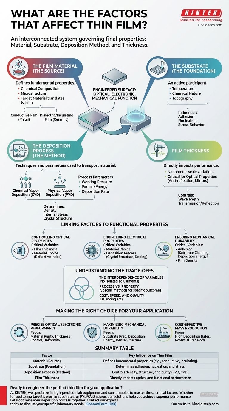
In essence, a thin film’s final properties are governed by a combination of four critical elements: the material being deposited, the substrate it is applied to, the precise deposition method used to apply it, and the final thickness of the film. These factors are not independent; they form an interconnected system where a change in one variable can significantly alter the others and the final outcome.
A thin film is not merely a coat of paint. It is an engineered surface where the choice of material, the nature of the substrate, and the physics of the deposition process must be precisely controlled to achieve a specific optical, electronic, or mechanical function.
The Pillars of Thin Film Engineering
To truly understand what affects a thin film, you must see it as a system with three core pillars: the material you are using, the foundation you are building it on, and the method you are using to build it.
The Film Material (The Source)
The inherent properties of the source material—often called the target material in sputtering processes—are the starting point for the film's characteristics. This is your primary choice for defining the film's fundamental nature.
The chemical composition and microstructure of the target material directly translate to the deposited film. A metal target will produce a conductive film, while a ceramic target will produce a dielectric or insulating one.
The Substrate (The Foundation)
The substrate is not a passive surface; it is an active participant in the film's formation. Its properties dictate how the film begins to grow, how well it adheres, and how it behaves under stress.
Key substrate characteristics include its temperature, chemical nature, and topography. These factors directly influence adhesion and the initial nucleation—the process where the first atoms or molecules begin to form islands of growth on the surface.
A mismatch in properties, like the rate of thermal expansion between the film and the substrate, can create internal stress, causing the film to crack or peel.
The Deposition Process (The Method)
The deposition process is the set of techniques and parameters used to transport the material from the source to the substrate. This is often the area with the most variables to control and optimize.
There are two primary families of deposition technology:
- Chemical Vapor Deposition (CVD): Uses precursor gases that react and decompose on the substrate surface to form the film. The final properties are controlled by gas flow rates, temperature, and pressure.
- Physical Vapor Deposition (PVD): Involves physically transferring material, for instance by evaporating a source (evaporation) or bombarding a target with ions to dislodge atoms (sputtering).
Within any chosen method, a host of process parameters must be precisely managed. These include the working pressure, the energy of the depositing particles, and the overall deposition rate. These variables determine the film's density, internal stress, and crystal structure.
Linking Factors to Functional Properties
The goal of controlling these factors is to produce a film with specific, predictable properties.
Controlling Optical Properties
For applications like anti-reflection coatings or mirrors, controlling film thickness is paramount. Thickness variations on the scale of nanometers can change which wavelengths of light are transmitted or reflected. The material choice determines the film's refractive index, another critical optical variable.
Engineering Electrical Properties
To create conductive pathways or insulating layers, the material choice is the primary factor. However, the deposition process can also be used to fine-tune conductivity by controlling the film's crystal structure or intentionally introducing impurity atoms in a process known as doping.
Ensuring Mechanical Durability
A film’s durability and scratch resistance depend heavily on its adhesion to the substrate and its internal density. Strong adhesion is promoted by careful substrate cleaning and choosing a deposition process that imparts high energy to the arriving atoms, embedding them securely onto the surface.
Understanding the Trade-offs
Engineering a thin film is a balancing act, and being aware of the inherent trade-offs is critical for success.
The Interdependence of Variables
You cannot adjust one parameter in isolation. For example, increasing the deposition rate to improve manufacturing throughput might decrease film density, making it less durable. Lowering substrate temperature to protect a sensitive component might result in poor adhesion.
Process vs. Property
Some deposition methods are better suited for specific outcomes. Sputtering, for example, generally produces denser films with stronger adhesion than thermal evaporation. However, it can also be a slower and more complex process. The ideal method is always a function of the application requirements.
Cost, Speed, and Quality
High-throughput, low-cost methods may not provide the fine control over thickness uniformity or material purity required for high-performance optical or electronic devices. The required performance level of the film will dictate the complexity and cost of the manufacturing process.
Making the Right Choice for Your Application
Your final decision must be guided by your primary goal.
- If your primary focus is precise optical or electronic performance: Your critical variables are material purity and exacting control over film thickness and uniformity.
- If your primary focus is maximizing mechanical durability: Prioritize substrate preparation, deposition energy, and process parameters that promote strong adhesion and a dense film structure.
- If your primary focus is cost-effective mass production: The choice of deposition method becomes central, favoring techniques with high deposition rates while understanding the potential trade-offs in film quality.
By understanding these fundamental factors, you can move from simply specifying a coating to intentionally engineering a functional material surface.
Summary Table:
| Factor | Key Influence on Thin Film |
|---|---|
| Material (Source) | Defines fundamental properties (e.g., conductive, insulating). |
| Substrate (Foundation) | Determines adhesion, nucleation, and stress. |
| Deposition Process (Method) | Controls density, structure, and purity (PVD, CVD). |
| Film Thickness | Directly impacts optical and functional performance. |
Ready to engineer the perfect thin film for your application?
At KINTEK, we specialize in providing the high-precision lab equipment and consumables you need to master these critical factors. Whether you require sputtering targets for specific material properties, substrates with precise characteristics, or expert advice on PVD and CVD processes, our solutions are designed to help you achieve superior optical, electronic, and mechanical performance in your thin films.
Let's optimize your deposition process together. Contact our experts today to discuss your specific laboratory needs!
Visual Guide
Related Products
- Aluminized Ceramic Evaporation Boat for Thin Film Deposition
- Tungsten Evaporation Boat for Thin Film Deposition
- Electron Beam Evaporation Coating Oxygen-Free Copper Crucible and Evaporation Boat
- Molybdenum Tungsten Tantalum Evaporation Boat for High Temperature Applications
- Aluminum-Plastic Flexible Packaging Film for Lithium Battery Packaging
People Also Ask
- What are thin films deposited by evaporation? A Guide to High-Purity Coating
- What is thin film deposition? Unlock Advanced Surface Engineering for Your Materials
- What is the source of evaporation for thin film? Choosing Between Thermal and E-Beam Methods
- Why is an alumina boat and Ti3AlC2 powder bed necessary for Ti2AlC sintering? Protect MAX Phase Purity
- Why is an alumina boat selected for catalyst precursors? Ensure Sample Purity at 1000 °C


